This thread has been locked.

If you have a related question, please click the "Ask a related question" button in the top right corner. The newly created question will be automatically linked to this question.

SN74LVC1G17: SN74LVC1G17

Part Number: SN74LVC1G17
Other Parts Discussed in Thread: ASH

Tool/software:

Hi,

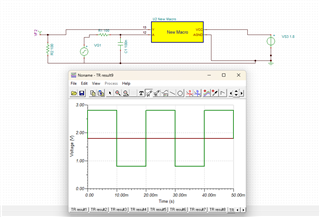
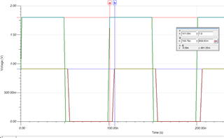
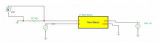
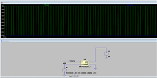
We are planning to use above part to provide delay upto 8ns. I am trying to do simulation but not able to see result as expected.

Any one can help me in simulation or let me know if any mistake in this below simulation.

Thanks

Ash

  • The propagation delay is less than 8 ns; you should add an R-C low-pass filter at the input to slow the edges of the input signal down.

    TI does not support LTSpice; I do not know if that model correctly simulates the propagation delay.

  • Ash,

    SPICE models are made to roughly simulate parameters like propagation delay but it's not going to be exact. I agree with clemens, you should use an RC filter and then measure delay on a few sample devices to see if it produces what you want.

    Best,

    Malcolm

  • Hi Clemens, Malcolm,

    Thanks a lot for reply. I have added RC also but didn't see any change.

    You are correct, I am using LTSpice. 

    I have downloaded TINA also, and added file as below and the simulation run. The output waveform comes as constant 1.8V. Ideally it should be same as input with some ns delay. Please let me know if any mistake I am doing.

    If you need design file, could you please share your email id. I am not able to add it here.

    Thanks

    Ash

  • Hi Ash,

    Not sure, you might have just not imported the part correctly, or it might have something to do with the way you connected the net at the output of the part. Here's what I get simulating on TINA, approximately a 6 nanosecond delay, no RC:

    Best,

    Malcolm

  • Hi Malcom,

    Thanks a lot for simulation.

    Could you please let me know why there is change in the input and output voltage. Ideally there should be same voltage between input and output.

    Thanks a lot helping here.

    Reagards

    Ash

  • The 100 Ω load would require an output current of 18 mA, which is much more than the recommended 4 mA. The 100 Ω and the buffer's output resistance form a voltage divider. If the output is to be connected to another CMOS input in the actual application, then 1 MΩ would be a better simulation.

    In your LTSpice simulation, the supply was 5 V but the input signal was never above 1.8 V, so it did never reach VIH.

    In your TINA simulation, the input signal appears to be between 0.8 V and 2.8 V. But it should be a digital signal between 0 V and 1.8 V.

    A buffer always outputs a digital signal at GND or at its own VCC.

  • Thanks a lot Clemens.