This thread has been locked.

If you have a related question, please click the "Ask a related question" button in the top right corner. The newly created question will be automatically linked to this question.

LSF0102: LSF VREFB control from 3.3V GPIO

Part Number: LSF0102

Hi,

We are planning to drive VREFB using a 3.3V GPIO, as suggested in the datasheet.
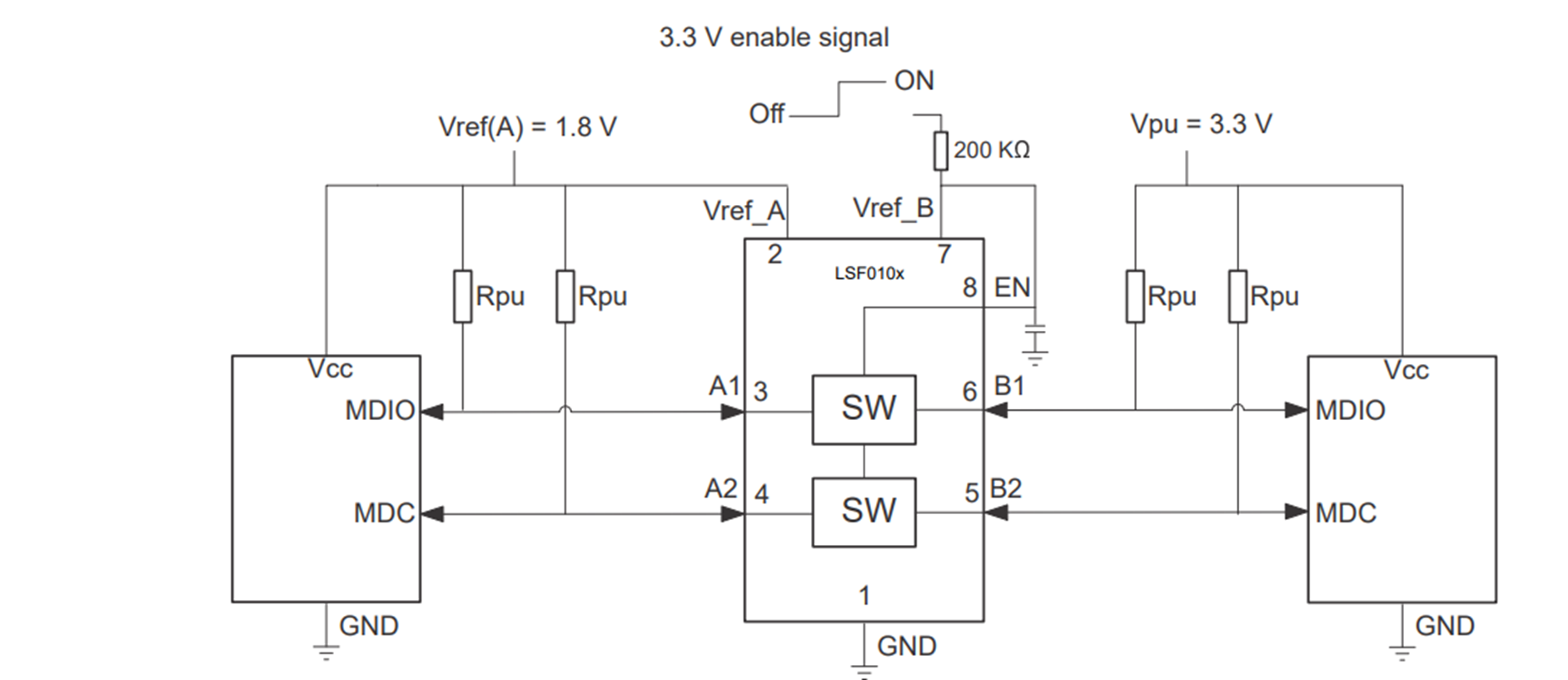
image.png

In our application, VREFA will be powered first, and VREFB will be driven later via the GPIO. As there is no specific power sequencing requirement mentioned, we would like to clarify the following:

  • Is the condition VREFB ≥ VREFA + 0.8V applicable only when the device is enabled (EN = 1)?
  • Or does this requirement also need to be maintained when the device is disabled (EN = 0)?

Could you please confirm the expected behavior in this scenario, particularly when VREFA is present while VREFB is not yet driven?

  • When EN is low, all I/Os are disabled, and the voltage at Vref_A does not matter.

  • Hi

    The VREFB ≥ VREFA + 0.8 V condition is required for proper biasing and level translation when the device is enabled (EN is HIGH).

    If VREFB/EN is not yet driven and EN is LOW, the LSF0102 I/O channels will remain in the high-impedance state, so no translation is expected during that time. The LSF family has no specific power-sequencing requirement, so VREFA may be present before VREFB, as long as the device is kept disabled until VREFB/EN becomes valid.

    The VREFB/EN node should not be left floating during this period; it should be held LOW if the device is intended to remain disabled.

    Thanks.