This thread has been locked.

If you have a related question, please click the "Ask a related question" button in the top right corner. The newly created question will be automatically linked to this question.

SN74LVCH16T245 Bus Hold

Other Parts Discussed in Thread: SN74LVCH16T245

Dear TI,

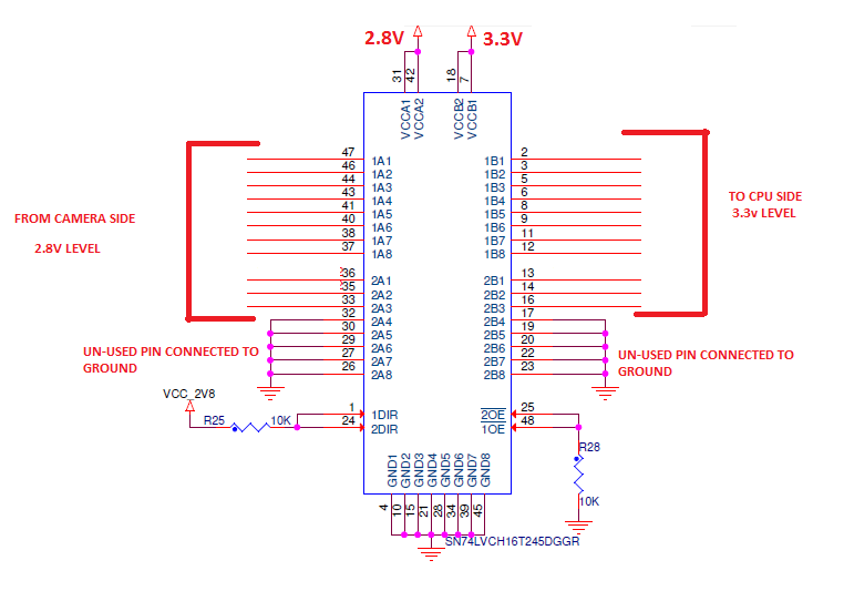
I'm using SN74LVCH16T245 for translating 2.8V camera signals to 3.3V camera signals. This IC has embedded with Bus-hold function. 

1. Please let us know, how to enable and dis-enable the bus hold function. 

2. Is it OK if I connected unused ins to ground ? 

3. Please review the circuit diagram and share the feedback. 

Regards,

Azlum

  • The datasheet says:

    The bus-hold circuitry on the powered-up side always stays active.

    Why do you think you need to disable the bus hold?

    Unused inputs should be connected to either VCC or ground. However, unused outputs should not be connected at all.

    The datasheet suggests a different configuration for the OE inputs:

    To ensure the high-impedance state of the outputs during power up or power down, the OE input pin must be tied to VCCA through a pullup resistor and must not be enabled until VCCA and VCCB are fully ramped and stable. The minimum value of the pullup resistor to VCCA is determined by the current-sinking capability of the driver.
  • Dear Guru ,

    With above circuit, I'm not getting any valid date at output side. It looks Bus-hold state.

    Regards,
    Azlum
  • This is not how bus hold works. Bus hold keeps the state of inputs that are not actively driven.

    How do the outputs look? High? Low? Hi-Z?

  • Output (Port B) looks Hi-Z state.
  • As per circuit diagram, here Unused pins (pin no 17 to 23) connected to ground. Is that OK ?
  • Tying the unused outputs to ground does not make sense, but should not hurt.

    R25 is superfluous, but should not hurt either.

    I'd guess that the problem might be that OE is low too early. As shown in my previous quote, it should be pulled high by default, and actively driven low later.

  • Hello Clemens Ladisch,

    OK.

    When OE is Low and DIR is High, A port is Hi-Z state. What does it mean ? This time A port will not accept any input signals ?

    Also please let me know what is Bus hold and when this feature is get enabled ?

    Regards,
    Azlum
  • The A ports are Hi-Z because they are inputs. This is normal.

    Read Application Report SCLA015: Bus-Hold Circuit.

  • Clemens - Thank you for taking the time to help out Mohammed.

    Mohammed,

    My responses to your questions are below:

    1. Please let us know, how to enable and dis-enable the bus hold function.

    Bus Hold is always enabled and it is a feature that is implemented on the input port. In your specific application, this means that if the camera decides to disconnect its outputs, the voltage on the 'A' pins would not drift off into an invalid voltage range (i.e. VIL < Pin Voltage < VIH). Bus Hold keeps the pin voltage within the valid range (i.e. Pin Voltage > VIH or Pin Voltage < VIL). If you had used a device that did not support Bus Hold, then under the same situation, you would need a pullup or pulldown resistor to guarantee a valid voltage on the 'A' pins. Without those pullups/pulldowns, a device that does not support Bus Hold would suffer from excessive device leakage.

    The camera should be able overdrive the Bus Hold as long as it can source/sink current that is above the IBHHO and IBHLO parameters listed in the datasheet. In your application, I would estimate +/- 500 uA.

    2. Is it OK if I connected unused ins to ground ?

    Yes, but it is not reccomended. For our devices that support Bus Hold, our recommendation is to leave unused pins open.

    3. Please review the circuit diagram and share the feedback.

    From what you have provided, your schematic connection should allow the translator to operate. I would prefer a complete schematic to review. I am assuming that you do not have any other circuit components connected other than the camera IC and the CPU IC.

    Have you checked the voltages on the DIR, !OE, VCCA and VCCB pins? Can you provide me with the voltage readings?

    For VCCA = 2.8V --> 1DIR and 2DIR should be > (0.7)*(2.8V) = 1.96V
    !1OE and !2OE should be < (0.3)*(2.8V) = 0.84V

    I would suggest that your force a DC voltage (High and Low) on the A pins, and see if that gets forwarded to the B pins (High and Low). For debug purposes, I try to verify DC translation first, then move onto AC translation.

    Best Regards,
    Nirav

  • Dear Nirav Patel,

    Thank you so much for the explanation.

    Here is the reading.

    1DIR, 2 DIR = 2.79V
    1OE, 2OE = 0V

    Regards,
    Azlum
  • Azlum,

    I would suggest the following next steps:

    Verify DC signal translation:

    1. Verify continuity from the camera pins to the Port A pins.
    2. Verify continuity from the Port B pins to the CPU
    3. Disconnect the camera, and apply a DC voltage (i.e. 2.8V) to the SN74LVCH16T245 pins 1A1 through 1A8. Double check that the actual voltage at these pins is actually 2.80V.
    4. Now measure the voltage on the SN74LVCH16T25 pins 1B1 through 1B8. It should be close to 3.30V.

    Best Regards,
    Nirav