This thread has been locked.

If you have a related question, please click the "Ask a related question" button in the top right corner. The newly created question will be automatically linked to this question.

SN74ALS541 output interface with another TTL device

Other Parts Discussed in Thread: SN74ALS541

Hello,

In Fig 1 Load Circuits and Voltage Waveforms on page 5 of the datasheet (SDAS025D, April 1982 - Revised March 2002), there are three load circuts: 1) RL from output to GND, 2) RL from output to Vcc, 3) R1 with S1 to 7V from output, and R2 from output to GND. 

In our design, the output of SN74ALS541 is going to connect to the input of a TTL device.  We have the following questions:

a) which load circuit should be used between the output of SN74ALS541 and the input of the TTL device: 1, or 2, or 3?

b) if the load circuit 3 is used between the two devices, could R1 connected to Vcc instead of 7V?

c) when R1 (560 ohm) is connected to Vcc, the VoH is jumping between 3.2V and 2.4V (see the attached file) , is this the expected outcome?
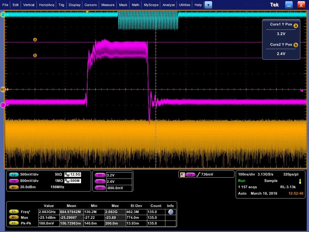
d) when the load circuit 1 (RL=560 ohm) is used, the VoH is jumping between 3.2V and 2.4V (see attached file), is this the expected outcome?

e) does this device have an output damping resistor?  If not, should that be ok to put a 25 ohm damping resistor between the output and the input of the next TTL device?

Best regards,

Mark Liang

  • Hi Mark ,

    The parameter information waveforms are in general for the SN74ALS series of devices . It is used to measure the timing parameters and the output behavior .
    1. You need not use any of the load circuit mentioned to connect the output of this device into TTL input .
    2 .If there needs to be valid output during OE assertion then either a pullup or pulldown needs to be used .
    3.4. Do you have plots for Vcc behavior ? any disturbance on Vcc can affect the outputs . Having a bypass cap close to Vcc pin could help . Having higher Rpullup resistor can help by lowering the load .
    This device does not have output damping resistor but there are other devices with internal output damping resistors like LVT2 ALVC2,ALS2 series. The output damping help in lowering the output drive and balancing signal impedance mismatch thereby reducing the overshoots /undershoots .
  • Hi Shreyas,

    Thank you very much for the reply.  

    What is the value of the bypass cap for Vcc, which you could recommend?

    Also, in my previous email, I was asking: "if the load circuit 3 is used between the two devices, could R1 connected to Vcc instead of 7V?", could you let us know, if you please let us know the answer for it?

    Thanks,

    Mark

  • Hi Mark ,

    In general , the bypass caps recommendation would be 0.1uF very close to the Vcc pin. you can also have multiple bypass caps(10nF/1nF/10uF ) across Vcc to reject different noise frequencies.
    yes , you can connect to R to Vcc and will work as load perfectly.