Hi,
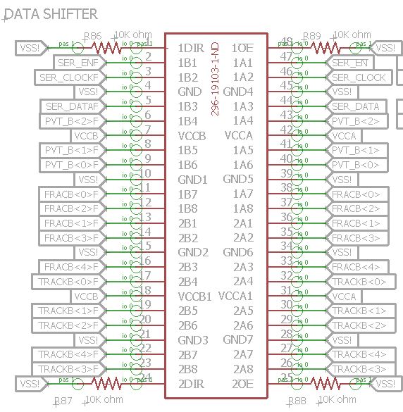
We are using SN74AVCH16T245 for the bidirectional translation between 1.2V signals (A side) and 2.5V signals (B side). A pull up resistor of 10Kohm has been used to tie OE to VCCA, which is 1.2V, with a control enabling a zero voltage while using the transmission function. Also, a pull down resistor of 10Kohm has been used to tie DIR to GND. B side is fed in the signals from a FPGA with a voltage level of 2.5V, which is the same as VCCB. VCCA (1.2V) and VCCB (2.5V) are powered on simultaneously. However, we can not get the chip to work properly in translating the signals from one side to another. It works after powering up and staying in tristate mode. When the OE was tied directly to GND by the control signal, while FPGA holding the signals to either high or low, it consumes more than 4mA and VCCA dropped to approximately 0.4V. How can I correctly configure the chip and get it wot work? Is it possible to directly tie the OE and DIR to either VCCA or GND for the bidirectional signal translation between 1.2V (VCCA) and 2.5V (VCCB)?
Thank you.