This thread has been locked.

If you have a related question, please click the "Ask a related question" button in the top right corner. The newly created question will be automatically linked to this question.

SN74AUP1G08: Max input rise/fall rate

Part Number: SN74AUP1G08
Other Parts Discussed in Thread: SN74AUP1G17, SN74AUP1G57, SN74LVC2G17

Hi,

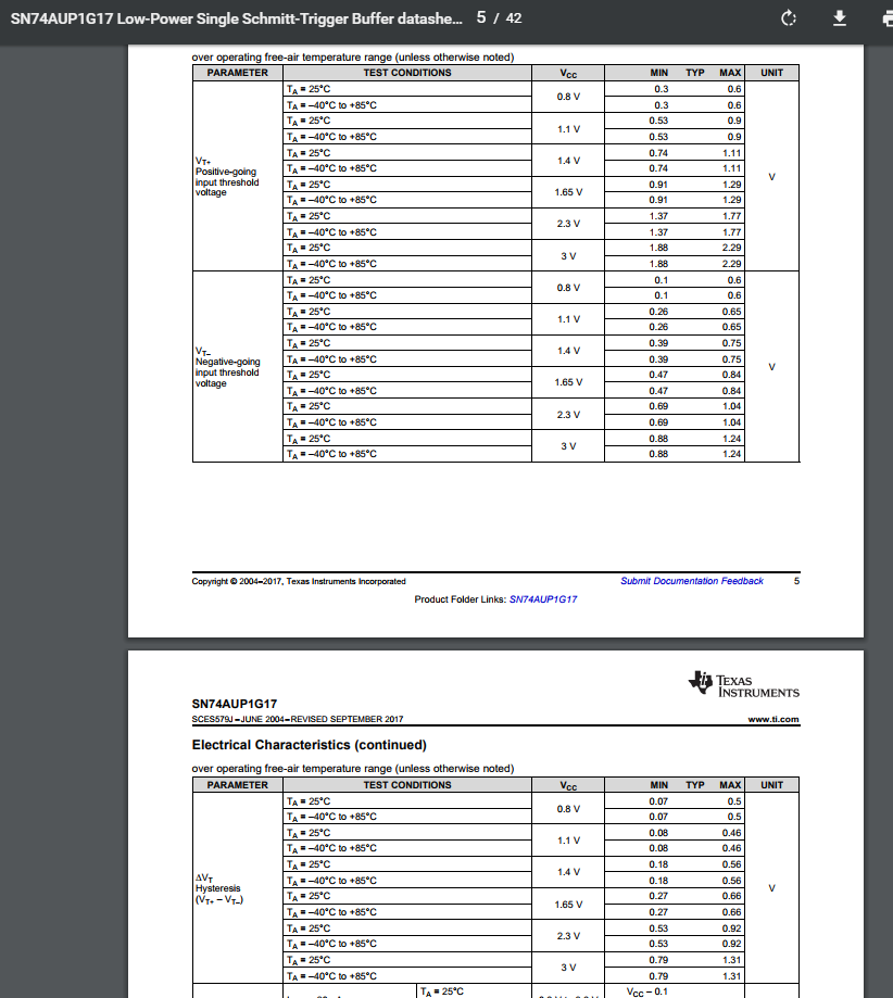
We see the max input rise/fall rate is 200nS/V in datasheet.  NOrmally 20uS/0V~3.3V should beover our spec, but customer said it's still working ell on their board.  Please provide your comments.

THanks!

Antony

  • Hello,
    Our response will be delayed due to the holidays.
  • Hello Antony,
    Our devices will often work when operated outside of the datasheet specs, but we do not guarantee that operation.
  • Hi Emrys,

    Thanks for your reply.  I see from datasheet that this chip support Schimit trigger, and it should be ok for slow input transition, right?

    Thanks!

    Antony

  • Hi Antony,

    This device is not a true Schmitt-trigger.  The marketing term "Schmitt-trigger action" refers to the improved spec in the recommended operating conditions:

    Many CMOS devices require less than 5 ns/V edge rates, over which this isclearly an improvement.

    The inputs to the SN74AUP1G08 should be faster than 200 ns/V.

    A true Schmitt-trigger device, such as SN74AUP1G17, will have threshold values listed in the electrical characteristics table like this:

    And that device can have very slow inputs.

    If you need an AND gate with Schmitt-trigger inputs, I would recommend looking at the SN74AUP1G57.

  • Hi Emrys,


    Thanks for your comments.


    Customer would like to know better about the risk using SN74AUP1G08 for their application. 

    The source of the two inputs to this AND gate is as below.

    1. Powergood signal (open drain with 10K PU to 3.3V) from a power chip.
    2. It comes from a SCHMITT-TRIGGER BUFFER with input from another controller reset pin (open drain).

    Considering the slew rate of above two signals could be slow as 20~30us as mentioned previously.  What is the worst case of the result?  Incorrect functionality?  SN74AUP1G08 damaged?


    Please also suggest which AND gate with Schmit Trigger function that you’ll suggest for them.


    Thanks!


    Antony

  • Hi Antony,
    I can think of two 'worst case' scenarios for a slow input. One would be output oscillations, causing multiple triggers (possibly hundreds or even thousands for a single edge). The other would be damage to the device from shoot-through current.

    You can read more about the effects of slow inputs here: www.ti.com/.../scba004d.pdf

    As for suggesting a part, I already did -- the SN74AUP1G57
  • HI Emrys,

    SN74AUP1G57 is a multi-function gate. So, we don't have a simple AND gate with Schmit Trigger inputs, right?

    Thanks!

    Antony
  • No - the only devices that have both the AND function and Schmitt-trigger inputs are the '57 configurable gates (and the '99 "super-configurable" gate)
  • Hi Emrys,

    May I know if SN74LVC2G17 a real Schimit Trigger buffer?  Customer's idea is to pass the signal to SN74LVC2G17 firstly, and then route it to the input of SN74AUP1G08?  Or should they use  SN74AUP1G17 (as you mentioned before) instead of SN74LVC2G17?  If SN74LVC2G17 is not workable for this, do we have a dual Schmit Trigger buffer?

    THanks!

    Antony

  • Hey Antony,
    Yes, the '17 function is a real Schmitt trigger and can be used as described (although I'm not sure why they would go for the 2 device solution instead of a single device solution with the 1G57). If you ever have a doubt, check the Electrical Characteristics table for a VT+ and VT- specification -- only Schmitt-trigger inputs will have those values specified in the datasheet.