Because of the Thanksgiving holiday in the U.S., TI E2E™ design support forum responses may be delayed from November 25 through December 2. Thank you for your patience.

This thread has been locked.

If you have a related question, please click the "Ask a related question" button in the top right corner. The newly created question will be automatically linked to this question.

CD40107B: CD40107B compatibility with CD4011B

Part Number: CD40107B
Other Parts Discussed in Thread: CD4011B, , SN74LVC2G00

I prototyped a momentary switching circuit using the CD4011B and it worked as intended, according to Fig.5 of this site.  Now, in the interest of reducing PCB area, I ordered the CD40107B instead of the CD4011B, since it has dual 2-input NANDs instead of quad.  When I assembled the PCB though, the circuit did not work.  I see on the datasheet that the CD40107B has some transistors on the outputs of the NAND gates, so I'm thinking this might be the cause of the incompatibility. 

Would I be correct in my determination, or do you think these two models are indeed compatible, and therefore interchangeable?

Or perhaps there is some extra circuitry I would need to add to the CD40107B's to make it work? 

I already ordered a bunch of PCB's, so I want to try and make it work.

Thanks!

  • Hi Fedor,
    The CD40107B has open-drain outputs - ie they cannot drive HIGH at the output on their own. If you want the CD40107B to work, you will have to add a pull-up resistor to the output of each. A 1k resistor would probably work for your circuit (I'm not 100% sure which circuit on that site you're using, but most used 100k's, so 1k should be fine).

    Have you considered something like the SN74LVC2G00? It comes in _much_ smaller packages to save space (assuming you can operate at <= 5V and don't mind soldering surface mount components).
  • Emrys,

    I am using the circuit in Fig. 5 of that link.  I tried 1K resistors, and the switch would not work at first, so I tried 10K resistors, and then the switch turned on!  However, the switch will not turn off.  I'm assuming this is because the output of the CD40107B that is driving the gates of the FET's (external to the CD40107B) are also now tied to Vcc (12 V in my circuit), so it just stays HIGH and cannot turn off?

    The SN74LVC2G00 looks like a viable option, except that my supply voltage to that CD40107B right is now is 12V, so I will have to at least add a resistor divider to make this work, and at that point is too many modifications, so I will need to just redesign.

  • A common technique is to complete your basic logic functions at 5V or 3.3V, then translate at the last stage to 12V using a discrete mosfet or BJT.

    From the circuit I saw, I don't see a reason why the circuit shouldn't work with a pull-up resistor. What is the second NAND gate driving at the output? You might have to reduce the pull-up resistor size to drive enough current... and that will produce a lot of stand-by current.
  • The second NAND gate is driving an IRFS7730TRL7PP MOSFET at the output.  I have tried testing it again, and now no matter if I use 1K, 10K, or 100K resistors, the switch neither turns on or off. 

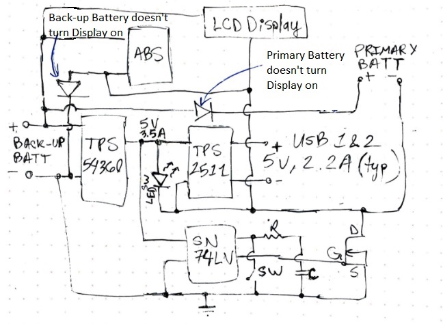
    If I am to redesign this circuit, I will use the SN74LV chip, as you are suggesting.  See below for high-level schematic of the design I have in mind:

  • It's possible that the slow edge on the power mosfet caused it to be damaged during turn-on. It's generally recommended to drive the gate of a power mosfet with a gate driver (ie push-pull high current drive output) rather than a weak driver (like you get with an open-drain device).

    From the mosfet datasheet, it looks like you can get away with a 5V logic circuit to drive the gate directly. The SN74LVC2G00 would likely do the trick.