This thread has been locked.

If you have a related question, please click the "Ask a related question" button in the top right corner. The newly created question will be automatically linked to this question.

SN74AVC2T45: 74AVC2T45

Part Number: SN74AVC2T45
Other Parts Discussed in Thread: SN74AXC4T245, SN74AXC1T45

Hello,

I have a query on the SN74AVC2t45 device. I understand from datasheet that when no vcca or vccb or both the I/o are in high impedance.

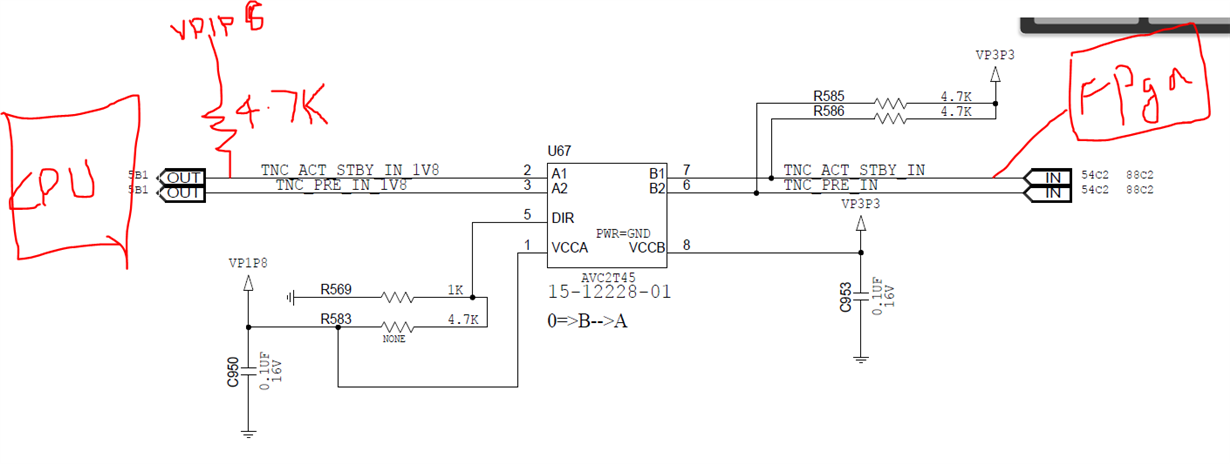
I am seeing a different behaviour in the implementation of our circuit. So, I would like to understand the reason. I am attaching the schema for reference.

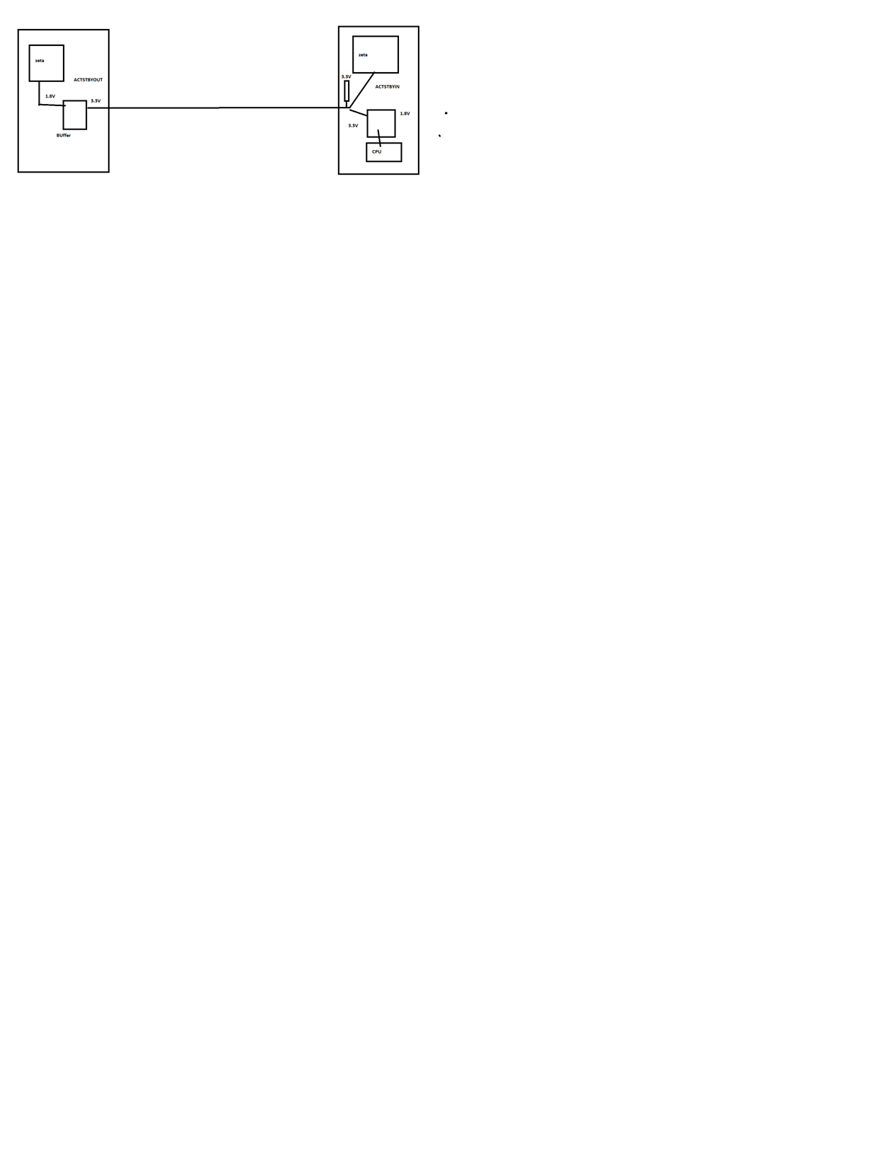
There are 2 cards in our system which are connected by the control line through the buffer ( AVC2t45).  The signal runs from card A to card B.

1. When we do power cycle of card A, we see that buffer output goes low immediately with 3.3V. Should it be holding high as we have the pull up on the card B?

2. How is the sink current getting the path when the 74AVC2t45 has a high impedance  because the supplies are going down.

Let me know if I need to be clear on. I can give some more explanation.

  • Hi Kamesh,

    Do you have a scopeshot of what you are seeing and what was the expectation? if you can also send the schematic that will help too.
    I assume that the DIR is set for A to B, but once the Vcca goes down, the DIR pin is low too.
    The device is not in Hi-Z until supply is about less than <0.5V.
    At that point, the device goes into hi-Z, and both channels are disconnected from each other.
  • Hi Shreyas,

    Thanks for the email. I am attaching the waveform for the power cycle command .

    During power cycle command.  The pink signal is the one we are talking about. The yellow and green are 3.3V and 1.8V respectively, The 3.3V and 1.8V seems to have leakage and it is not fully 0.

    We don't see the issue during OIR, which is removal and insertion of card back..Here you can see pink one is stable high. The 3.3V and 1.8V still have leakage but probably below 0.5V.

    schematic

    Let me know if you need more information.

    Thanks

    Kamesh

  • Hi Kamesh,

    Was there a schematic to be attached in the post?
    You can click on the Insert Code, attach files link to your right and post it.
    If the low level is not exactly or close to 0V, then there is some output loading, usually like the pull-up resistor, which causes current to sink into the device thus raising the low level above 0V.
  • Hi Shreyas,

    I had pasted the snapshot like the one below. So can I understand this way if the VCCA or VCCB or not 0V , it may not keep the  lines in high impedance . Is that correct?. What is the threshold voltage at vcca or vccb that helps keeps the lines in high impedance,

    Thanks

    Kamesh.

  • Hi Kamesh,

    Thanks for the schematic.
    I hope that the 1K resistor is not populated.
    You are right, the Ioff is guaranteed only when Vcc is held at gnd level till about 0.1V threshold when the device IO ports become active. Leaving the device pin floating will not ensure hi-z.
  •  Hi Shreyas,

    The 1K res is not populated. I would like to share the other part. The B1 output of the U66 chip goes to other card which is not power cycled. We have a pullup there to 3.3V and that gets connected to FPGA. I have enclosed the schematic. I hope it is clear.

    1. If I remove the R586 resistor, will I be able to control the leakage?

    2. Since the direction of u67 is B to A.and power is stable in this card, I should not see the leakage coming from the 1.8V pull up side.

    Please confirm.

    Thanks

    Kamesh.

  • Kamesh,

    If the B1 is supposed to be default held high during Hi-Z or power up /power down (Vcca or Vccb), you could replace the 4.7K pullup with 50K/100K. This will limit the leakage current and will help to have the output close to 0V low level during normal operation as you had initially described in your second post.
    There should not be leakage from the A to B side (or from Vcca---> Vccb) once the device is disabled or during operation.
    Let me know if anything else.

    Have you considered using the SN74AXC1T45 or the SN74AXC4T245 which we recently released? Refer to my signature below for more information on it.