This thread has been locked.

If you have a related question, please click the "Ask a related question" button in the top right corner. The newly created question will be automatically linked to this question.

SN74AUP1G14: questions

Part Number: SN74AUP1G14

Hi Expert,

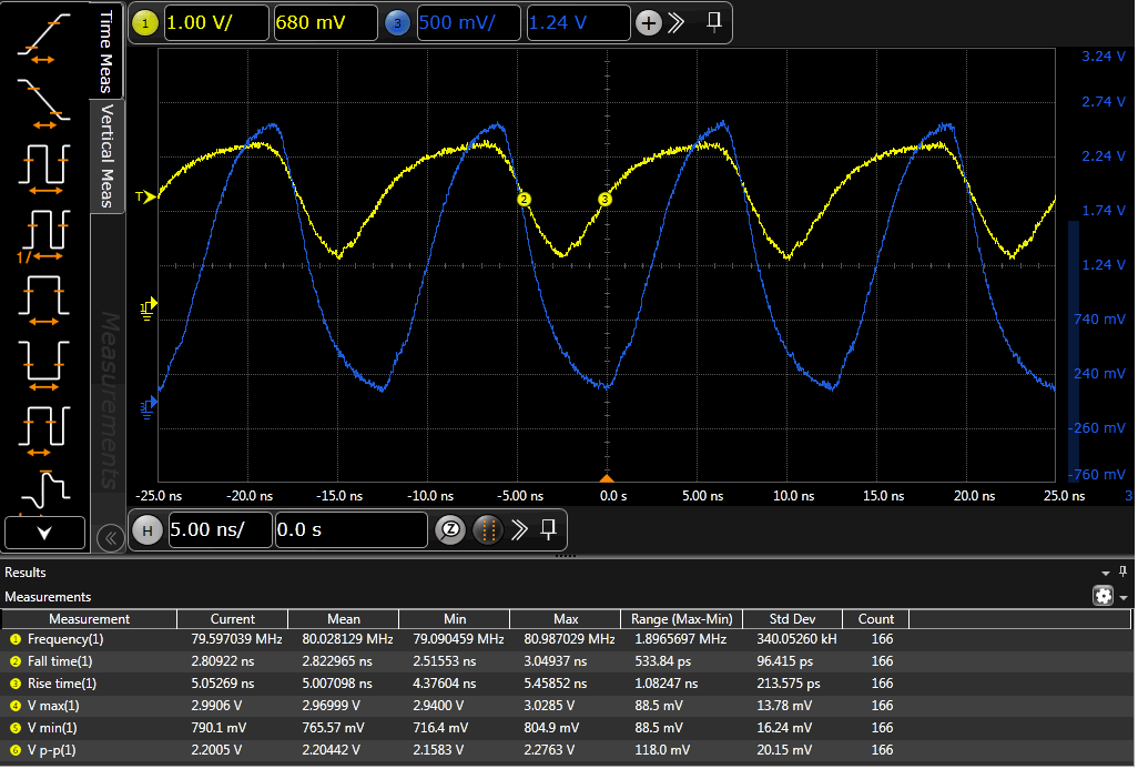
We are replacing NC7SV14P5X with p2p SN74AUP1G14 but the input/output signals looks distorted. Would you please have a look and let us know if any suggestions? 

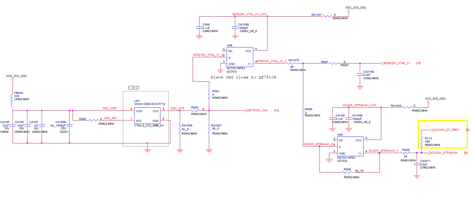
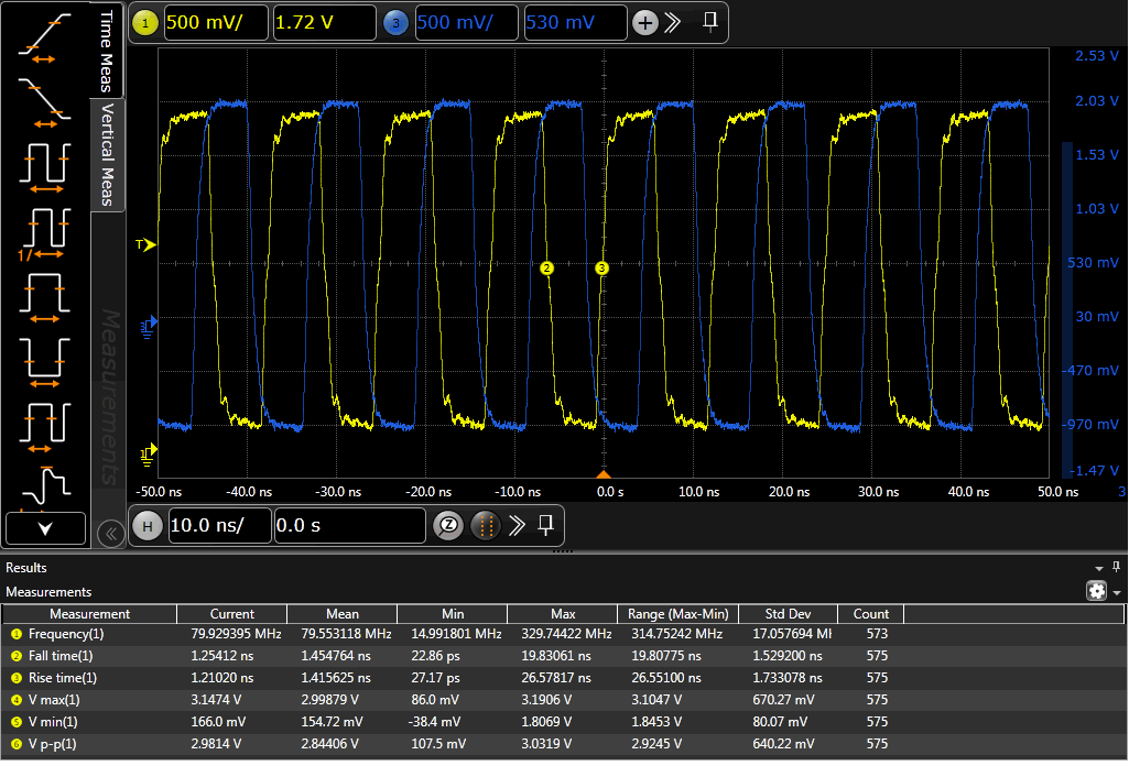
Original input(Blue)/output(Yellow)waveform of NC7SV14P5X 

input(Blue)/output(Yellow) waveform of SN74AUP1G14 

Thanks,

Allan

  • The input signal is quite different.

    There are two inverters in the circuit. What points were measured?

    And the propagation delay looks funny. Is blue really the input?

  • Hi Clemens,

    Thanks for your reply. Sorry we didn't explain clearly. The in/out customer measured is at UA8 pin2 and pin4 so maybe the signal is somehow distorted already from UA6. They will measure the in/out on UA6 and update afterward. 

    Besides that, may I know what's the maximum clock frequency that SN74AUP1G14 can support? Cause customer would use 80Mhz.

    Regards,

    Allan  

  • UA8 has capacitors at its input and output, and there negative feedback. What is the purpose of RA99?

    The maximum frequency is limited by the output drivers. The graphic below shows the maximum input clock for a flip-flop, so for a buffer, the maximum frequency is half that. 80 MHz is at the limit (for a device without additional capacitive loads). At 2.5 V, it would be possible to use AUC.