This thread has been locked.

If you have a related question, please click the "Ask a related question" button in the top right corner. The newly created question will be automatically linked to this question.

CD4047B: Parasitic oscillation

Part Number: CD4047B
Other Parts Discussed in Thread: TPL5110

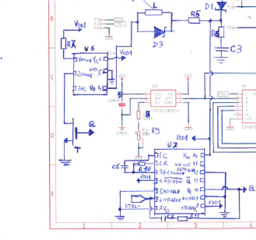
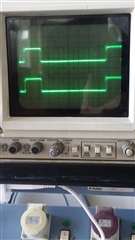
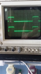
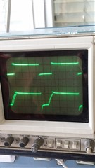
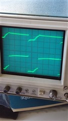
I'm designing a circuit in which the Q output of CD4047BM drives a MOSFET gate whose drain drives a relé coil, powered by a 1 F supercapacitor at 5 V; the CD4047BM is triggered by -TRIGGER input. During power on, with 5 V power supply voltage, a parasitic oscillation arises, also if the CD4047BM is still not triggered; the oscillation involves also the relé coil, and the vibration noise is heard. Oscilloscope measurements give 3 to 5 ms period of the produced oscillating square wave. Please, could you indicate how to avoid this? Thank you very much.

  • Hi,

    Could you provide us with a schematic and scope shots of the issue you're seeing?

    Thanks!

    Chad Crosby

  • Dear Dr. Crosby,

    thank you for your answer.

    I hope you are well.

    I tried to insert the schematic of the circuit but the system didn't accept  it.

    Please, could you send me an email address to send you it?

    My best regards

    Salvatore

  • To insert an image or file, use the Insert▼Image menu at the bottom.

  • Hi Salvatore,

    E2E was recently updated to allow drag and drop support for images. If you have a picture of your schematic, you can simply drag and drop it into the text box. If you have a file to add, you'll need to use the insert tool at the bottom of the text box.

    Thanks!

    Chad Crosby

  • Hi, here is the schematic of the circuit

    U7 is CD4047BM; U6 is a Schmitt trigger optocoupler; T is a MOSFET; Q output from U7 drives the T gate; C3 is charged at 5 V; the -TRIGGER signal is provided by the negative going J output of the OR gate U4.

    Thank you very much.

    My best regards

    Salvatore

  • Hi Salvatore,

    It's kind of hard to see this schematic. Do you have it in PDF format, or in a higher resolution jpg? Also, do you have any scope shots immediately at the pins of the device?

    Where are you seeing the parasitic oscillation? Is it at the output of the device, or is it being fed into the device? It would help me greatly if you could attach a clear image/pdf of your schematic and any scope shots you have.

    Thanks!

    Chad Crosby

  • Hi dr. Crosby

    here is an high resolution pdf of the schematic.

    Monostabile.pdf

    I'm sorry at the moment I have no shots. 

    U7 is CD4047BM; U6 is a Schmitt trigger optocoupler; T is a MOSFET; Q output from U7 drives the T gate; C3 is charged at 5 V; the -TRIGGER signal is provided by the negative going J output of the OR gate U4.

    I see the coil is drived by an about 5 ms period square wave.

    My best regards

    Salvatore

  • Hi Salvatore,

    I still don't think I have enough information to help solve this problem. I think a scope shot at pin 6 of U7, as well as a scope shot at pin 10 of U7 will be the most helpful for me to understand why this problem is happening.

    At the most, all I can do right now is guess why you might be seeing what you're seeing:

    1. First and foremost, I wouldn't recommend trying to use a logic device as a gate driver. This device has a pretty weak current driving capability (~1mA push/pull). I'm not sure what the specs are of the FET you're trying to drive because the schematic you provided seems limited, but this would be my first place to start looking.

    2. It could noise coupling into the power supply rail. I see that you have a 1F supercap acting as your supply, but I also recommend having a smaller decoupling cap (100nF or so) at the supply pin of U7, as well as U4 (if one isn't there already)

    3. What is the purpose of the feedback RC from pin 10 to 6 of U7? Have you tested this circuit with these components removed?

    Again, if you can provide me with some scope shots & a more detailed schematic that would be most helpful - otherwise, I'm not sure there's much else I can do.

    Thanks!

    Chad Crosby

  • Dear dr. Crosby,

    thank you for your interesting answer.

    I've understood your network study needs, and I made some scope shoots.

    I applied also suggestion #2 in your previous message. In this measurements C7 = 10 nF, R11 = 10 kOhm. Here is a synthesys of my work:

    1) Photo 1 and 2


    Photo 1                              Photo 2

    Channel #1 (upper trace) : pin 6 U7 (CD4047BM), 2 V/div; Channel #2 (lower trace) : pin 10 U7, 2 V/div; X: 0.5 ms/div.

    The -TRIGGER pin was disconnected by the J output of U4 CD4072BM; the -TRIGGER pulse was produced by a ground-connecting manual switch. U7 VDD pin had a 100 nF decoupling cap.

    Oscillations arise during 1F C3 supercap charging, then they stops; after C3 charging there are no more oscillations, also after CD4047BM triggering.

     In the next post 2 scopes for the whole circuit.

    Thank you

  • 2) Photo 3

    Photo 3 (The system didn't allow to drop the image)

    Channel #1 (upper trace) : 5V output of the power line of the relè (not seen in the schematic), driven by the L coil, 2 V/div; Channel #2 (lower trace) : J output U4, 0.5 V/div; X: 1 ms/div.

    The -TRIGGER pulse is given by the J output of U4; the previously used manual switch was removed. Both U7 and U4 VDD pins had a 100nF decoupling cap. 

    Oscillations arises during C3 charging. The J output should be a long-lasting (1 h) low level without oscillations.

    3) Photo 4

    Photo 4 (The system didn't allow to drop the image)

    Channel #1 (upper trace) : pin 6 U7, 1 V/div; Channel #2 (lower trace) : pin 10 U7, 1 V/div; X: 1 ms/div.

    The -TRIGGER pulse is given by the J output of U4; the previously used manual switch was removed. Both U7 and U4 VDD pins had a 100nF decoupling cap. 

    I hope to have success in inserting photos in another post tomorrow.

    Thank you very much.

    My best regards

    Salvatore

  • Here are answering to questions in your last post.

    1. The transistor T is the Vishay Si2302DDS N-channel MOSFET, whose input current with almost DC gate driving (f <<< 1 Hz) is about zero. I see several times logic gates driving MOSFETs (e.g. TI TPL5110 data sheet fig. p. 1).

    2. Probably oscillations arises in the power supply line; once I tried to remove the 1 F C3 and to substitute it by an external power supply; oscillations increased and lasted more.

    3. The purpose of the RC feedback from pin 10 to 6 of U7 is to limit noise effect on -TRIGGER input, as suggested by a book found in Internet describing in detail some IC, including CD4047Bm.

    Thank you again.

    My best regards

    Salvatore

  • Hi Salvatore,

    You might need to log out and log back into E2E in order to post images again, we've recently updated E2E, so there might still be a few bugs.

    Oscillations arise during 1F C3 supercap charging, then they stops; after C3 charging there are no more oscillations, also after CD4047BM triggering.

    What else do you have connected to this power rail? 

    I'll wait for you to post the scope shots of your noisy signals.

    Thanks!

    Chad Crosby

  • Hello dr. Crosby,

    I hope you are well.

    Here are the two other photos.

    2) Photo 3

    Photo 3 

    Channel #1 (upper trace) : 5V output of the power line of the relè (not seen in the schematic), driven by the L coil, 2 V/div; Channel #2 (lower trace) : J output U4, 0.5 V/div; X: 1 ms/div.

    The -TRIGGER pulse is given by the J output of U4; the previously used manual switch was removed. Both U7 and U4 VDD pins had a 100nF decoupling cap. 

    Oscillations arises during C3 charging. The J output should be a long-lasting (1 h) low level without oscillations.

    3) Photo 4

    Photo 4 (The system didn't allow to drop the image)

    Channel #1 (upper trace) : pin 6 U7, 1 V/div; Channel #2 (lower trace) : pin 10 U7, 1 V/div; X: 1 ms/div.

    The -TRIGGER pulse is given by the J output of U4; the previously used manual switch was removed. Both U7 and U4 VDD pins had a 100nF decoupling cap. 

    Thank you very much.

    My best regards

    Salvatore

  • Dear dr. Crosby,

    here is the answer to your question.

    C3 powers: the relé (nonshown in the schematic) coil L; U6; U7; all the rest of the circuit, including U3 and U4, is powered by another 1 F supercap placed exacly parallelly at C3 (both 1 F supercaps are charged by the sale power line, which they are decoupled from by a Schottky diode each).

    My best regards

    Salvatore

  • Hi Salvatore,

    I'm not sure how much I'll be able to help here, as it seems like there isn't an issue with our part here, but rather an issue with supply noise. I'll take a look at the above and get back to you when I can.

    Thanks!

    Chad Crosby

  • Hi Salvatore,

    What is the sizing of your timing components C6 and R10? You'll likely need to add more capacitance close to U7 in order to support the charging of the timing components. I think what might be happening here is you're being limited by the ESR of the super capacitor, and you might want some larger ceramics closer to the part (1uF or maybe more).

    Hope that helps,

    Chad Crosby