Hi All,
I have a question about SN74AVC2T45.
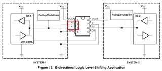
I think the figure in Figure 15. is wrong.
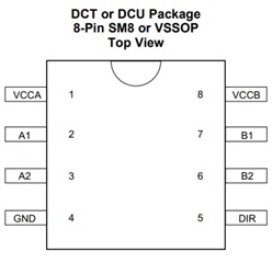
I think the positions of the A1 and A2 pins are opposite.

The correct terminal is understood below.
The connections are A1 and B1, which are understood as A2 and B2.
Is my perception correct?

Also, please tell me the processing for unused terminals.
Looking at Figure 15, it is directly connected to GND.
I think it is better to connect via a pull-up / pull-down resistor.
Best Regards,
Ishiwata

