Other Parts Discussed in Thread: SN74LVC1G123
FAQ: Logic and Voltage Translation > Output Parameters >> Current FAQ
The answer to all three questions is "yes" - these are the three primary uses of open-drain outputs on logic devices. Much of this also extends to open-collector devices, but they are much less common today due to the age of bipolar technology.
What is an open-drain output?
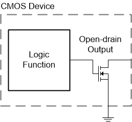
An open-drain output is basically just an n-channel MOSFET connected to ground at the output of the device. This MOSFET can either be turned ON, resulting in a relatively low impedance path to ground at the output, or it can be turned OFF, resulting in a very high impedance path to ground.
An open-drain device typically will use Hi-Z, or just Z, in the logic table to indicate when the output is in the high-impedance state, but there are some out there that just list "H" and expect the reader to know that "H" for an open-drain device means "Hi-Z."
Voltage Level Translation with an Open-Drain Buffer
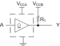
The most common use-case for an open-drain device is to do voltage level translation, as shown here:
The input voltage thresholds for the open-drain buffer are controlled by V_CCA, and the output high-level voltage is controlled by V_CCB. This is a very simple circuit to implement and is used in many applications, but it does have some drawbacks. The output can either be fast or low power, in this configuration both are not achievable at the same time. To be fast R1 must be very small, but that will result in a large amount of current draw from V_CCB. To be low power, R1 must be very large, but that will result in a slow rising edge that can be detrimental in many system. Usually a resistance between 1kohm and 10kohm is selected to balance these two issues.
Directly Connect Outputs with an Open-Drain Device
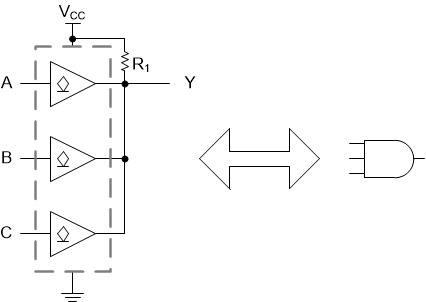
Another very common use-case for an open-drain device is to directly connect together outputs. This cannot be done with normal CMOS devices because the outputs can have opposing states and huge amounts of current can be created resulting in damage to the device or system.
With an open-drain output, there is no danger of one output being HIGH and another being LOW since all outputs are either LOW or Hi-Z. In the above image we show how three open-drain buffers can be combined to produce a 3-input AND gate function. It is important to note that the output signal has the same limitation as the previous use-case: the signal can either be fast or low power, but not both.
Discharge a Voltage Node to 0V with an Open-Drain Device
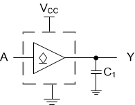
Sometimes it is beneficial to have a minimal impact on a voltage node during normal operation, but occasionally that node needs to be discharged.
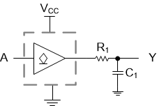
An example would be a timing capacitor - an open-drain device can be used to quickly discharge the capacitor, then it can be allowed to charge naturally when the open-drain device switches back into Hi-Z mode. Monostable multivibrators such as the SN74LVC1G123 use this type of circuit internally to discharge their timing capacitors, and systems can also use a similar technique for many applications.
If the capacitor is relatively large, it is possible to exceed the current ratings of the open-drain device, so a small resistor is added in series with the output to reduce the discharge rate:


