This thread has been locked.

If you have a related question, please click the "Ask a related question" button in the top right corner. The newly created question will be automatically linked to this question.

SN74LVC2G14: datasheet layout example

Part Number: SN74LVC2G14

Hello all,

I always like it when a datasheet provides layout hints.

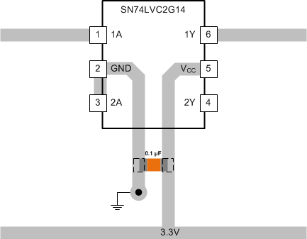
For the SN74LVC2G14, the datasheet shows the following layout example:

I assume that the 0.1 µF capacitor is meant to operate as a bypass capacitor to prevent power disturbances. However, I think this layout doesn't work as expected. What is Vdd?

I believe that the capacitor should be placed below the IC and connected to pin 2/3 and pin 5. Or am I missing something?

Thanks.

Daniel

  • Hi Daniel,

    Thanks for bringing this to our attention. I will mark this as an error in the datasheet for us to update in the future.

    You are correct that the 0.1 µF capacitor is intended as a bypass capacitor. This is definitely an error. The Vcc pin should be connected directly to the supply, and the capacitor should be connected from the supply pin to ground, as close as possible to the device.

    Here's a better example of a layout when one channel is not used:

  • Emrys,

    Thanks, your answer is very helpful.