AM263P2: the OSPI interface of the AM263P2 MCU

Part Number: AM263P2
Other Parts Discussed in Thread: AM2612, AM263P4

Tool/software:

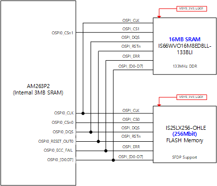
I'm planning to use the OSPI interface of the AM263P2 MCU as follows:

1. We plan to use the 16MB SRAM from ISSI for data logging via the OSPI interface CS1. (I understand this connection is slower than the SRAM inside the AM263P2, so I plan to use it for data reference purposes.)

- 133MB DDR CLK
- 3.3V power supply
2. We plan to use the 256Mbit flash memory from ISSI, which supports SFDP (Serial Flash Discoverable Parameters), via the OSPI interface CS0 for OS booting.
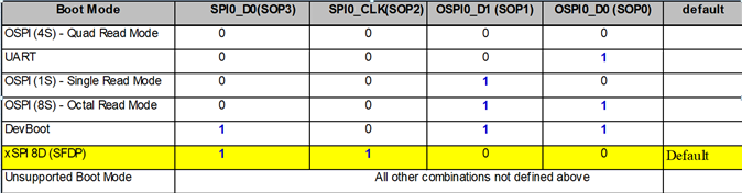
- MCU boot mode will be xSPI 8D (SFDP).
- 133MB DDR
- 3.3V power supply
3. We will use the OSPI signals in common, but use a separate chip select.

Question
1. Are there any issues with the circuit diagram?

2. Is there a problem with operating two components (SRAM and FLASH) simultaneously?

  • Hi Jongho Park,

    Apologies for the long delay!!

    Are there any issues with the circuit diagram?

    ISSI PSRAM cannot be used with AM263Px OSPI0 interface as it requires additional Address Translation logic. Instead you can use a APMemory PSRAM which doesn't require address translation.

    2. Is there a problem with operating two components (SRAM and FLASH) simultaneously?

    Can you please elaborate on the use case ? Since there are no separate configuration registers for 2 Chip Selects, SW needs to takecare of switching the configurations for PSRAM and FLASH which is quite tricky. And the program during the switching should be executed form RAM instead of Flash (as controller will be busy configuring the PSRAM).
    Hence in summary simultaneous operation is not supported

    Instead I would like to pitch you another device from the same family --> AM2612

    AM2612 is a dual core device which has 2 separate OSPI Controllers(OSPI0 \ OSPI1):

    1. OSPI0 - CS0 can be connected to ISSI FLASH for boot
    2. OSPI1 - CS0  can be connected to ISSI PSRAM. OSPI1 interface in Am2612 has additional Address translational logic extending its support to ISSI PSRAMs

    Please refer to section 13.3.5 Octal Serial Peripheral Interface (OSPI1) in Am261x TRM for more details.

    Thanks & Regards,
    Rijohn

  • Thank you for your reply.

    Our application requires an MCU with HW Safety Integrity Level SIL3 certification.
    We also require the following specifications:
    - CAN FD 2-channel
    - Flash Memory: Approximately 32MB (with ECC)
    - At least 16MB of DDR RAM with ECC (This part can actually operate with 2MB of SRAM, but the manufacturer's minimum requirement is 16MB or more. Therefore, we plan to operate with 2MB of SRAM and use the 16MB for logging data or debugging purposes only.)
    Currently, the AM26x series is SIL3 certified and does not have a separate DDR RAM interface, so we plan to use the OSPI interface to attach 16MB of SRAM.
    The AM263P2 (supporting lock step) supports 3MB of SRAM, and we plan to attach 16MB of PSRAM and 32MB of flash externally via OSPI.

    If I were to use the OSPI on the AM263P2 to connect FLASH memory (CS0) and SRAM memory (CS1) and operate them simultaneously, would it be possible to operate them separately from the upper-level application at runtime?
    Please let me know if I can use the circuit diagram I wrote above as is for the hardware configuration to make it work, or if I need to modify it.
    Also, please tell me how to make it work from a software perspective.

    See the E2E answer below:
    Nilabh Anand:
    "They can use it at runtime as well, if they can do proper handling at the application level."
    Link to answer:
    e2e.ti.com/.../am263p4-connecting-two-devices-to-ospi-interface

    Also, The AM2612 appears to have 1.5MB of SRAM. We need at least 2MB of SRAM.

    If there's an MCU like the AM2612 that supports two OSPI controllers, has at least 2MB of SRAM, and is SIL3-compliant, please recommend it.


    Thank you.

  • You are definitely not alone with this issue. We are working with the AM263P4 and run into similar limitations — having only ~3 MB shared between code execution and data is really restrictive.

    In our case, we don’t need high-speed random access for external data, so the only thing we can do is attach PSRAM over a regular SPI interface and handle it through a software driver (not memory-mapped by the controller). It’s a rather desperate workaround, but since there is no real alternative, it may still be acceptable for some use cases.

  • Hi Jongho,

    After thorough examination of your requirements, I would like to provide the following clarification:


    Technical Limitations:

    The OSPI interface on the AM263P2 utilizes a shared address and data bus architecture with device selection managed through individual Chip Select (CS) signals. Due to this hardware design constraint: Simultaneous operation of multiple devices (Flash and pSRAM) is not feasible through a single OSPI controller.


    Implementation Approach:

    While simultaneous operation is not possible, you can implement a sequential access methodology with the following considerations:

    1. Controller Configuration Management:

    • Each memory device type requires specific controller configuration parameters.
    • Flash memory operations utilize distinct command sets and timing requirements.
    • pSRAM operations necessitate different protocol configurations and access patterns.

    2. Runtime Switching Protocol:

                     When transitioning between Flash (CS0) and pSRAM (CS1), the application must:

    • Save current context if necessary.
    • Reconfigure the OSPI controller with appropriate parameters for the target device.
    • Execute the required memory operations.
    • Restore previous configuration if returning to the original device.

    Clarification of Previous E2E Response:

    Regarding the statement from the E2E forum: "They can use it at runtime as well, if they can do proper handling at the application level."

     This specifically refers to the requirement for implementing the aforementioned controller reconfiguration logic within your application. The "proper handling" entails managing the configuration transitions between devices during runtime operation to ensure correct protocol parameters are applied before accessing each respective memory device.


    Let me know if you need more clarification on this.

    Thanks & Regards,
    Mayank Shadwani