Other Parts Discussed in Thread: CONTROLSUITE
Hello All,
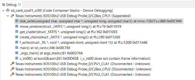
So, I have a requirement to log the data to SD Card periodically for some parameters. I started using the SD Card example provided in ControlSuite. I modified wc=0 to wc=256 in xmit_datablock function in mmc-F2837x.c file. I modified the main function and added function calls to f_mount, f_open, f_write, f_sync, f_close and f_mount in the sequence mentioned to create a file and write a string to it. I am able to successfully do that without any problems. No I am trying to implement DMA feature to SPI TX Channel but I am not able to do that successfully. I am using "Example_2837xD_Spi_dma" as an example for DMA use.
I want to write blocks of 512 bytes at a time using DMA. That way I dont need to heavily modify the code. So, here is the configuration and the changes that I made based on my understanding in the sd_card example.
I added the following in mmc-F2837x.c file:
#define BURST         (FIFO_LVL-1)    // burst size should be less than 8
#define TRANSFER      63              // [(MEM_BUFFER_SIZE/FIFO_LVL)-1]
#define FIFO_LVL      8               // FIFO Interrupt Level

//
// Globals
//
volatile Uint16 *DMADest;
volatile Uint16 *DMASource;
volatile Uint16 SpiTxDmaDone = 0;

// Function Prototype
void dma_init(void);
I added the following code in the power_on function again in mmc-F2837x.c file:
// SPI Port Settings
/* Configure the SPI C port */
SpicRegs.SPICCR.bit.SPISWRESET = 0;			//Set reset bit low
SpicRegs.SPICTL.bit.CLK_PHASE = 0;
SpicRegs.SPICCR.bit.CLKPOLARITY = 1;
SpicRegs.SPICTL.bit.MASTER_SLAVE = 1;		//Master mode
SpicRegs.SPIBRR.all = 63;					//update value to proper setting for correct bitrate ( current: ~500kHz)
SpicRegs.SPICCR.bit.SPICHAR = 0x7;			//Set char length to 8 bits
SpicRegs.SPICTL.bit.TALK = 1;
SpicRegs.SPICCR.bit.SPISWRESET = 1;			//Release SPI from reset
SpicRegs.SPIPRI.bit.FREE = 1;
SpicRegs.SPIPRI.bit.SOFT = 1;

EALLOW;  // This is needed to write to EALLOW protected registers
PieVectTable.DMA_CH5_INT= &local_D_INTCH5_ISR;
EDIS;   // This is needed to disable write to EALLOW protected registers

dma_init();            // Set up DMA for SPI configuration

SpicRegs.SPIFFCT.all = 0x0;

for(m=0;m<3;m++);

SpicRegs.SPIFFRX.all=0x2040;             // RX FIFO enabled, clear FIFO int
SpicRegs.SPIFFRX.bit.RXFFIL = 0;  // Set RX FIFO level

SpicRegs.SPIFFTX.all=0xE040;             // FIFOs enabled, TX FIFO released,
SpicRegs.SPIFFTX.bit.TXFFIL = FIFO_LVL;  // Set TX FIFO level

// Ensure DMA is connected to Peripheral Frame 2 bridge (EALLOW protected)
	EALLOW;
	CpuSysRegs.SECMSEL.bit.PF2SEL = 1;
	EDIS;

// Enable interrupts required for SPI DMA
	PieCtrlRegs.PIECTRL.bit.ENPIE = 1;   // Enable the PIE block
	PieCtrlRegs.PIEIER7.bit.INTx5 = 1;   // Enable PIE Group 7, INT 1 (DMA CH1)
	PieCtrlRegs.PIEIER7.bit.INTx6 = 1;   // Enable PIE Group 7, INT 2 (DMA CH2)
	IER= M_INT7;                         // Enable CPU INT6
One thing to note is that I have SpicRegs.SPICCR.bit.SPICHAR = 0x7 as sd_card example uses BYTE (unsigned char) type.
DMA Init and TX ISR looks like this:
//
// dma_init - DMA setup for both TX and RX channels.
//
void dma_init()
{
    //
    // Initialize DMA
    //
    DMAInitialize();

    //
    // configure DMACH5 for TX
    //
    // DMACH5AddrConfig(&SpicRegs.SPITXBUF,DMASource);
    DMACH5BurstConfig(BURST,1,0);         // Burst size, src step, dest step
    DMACH5TransferConfig(TRANSFER,1,0);   // transfer size, src step, dest step
    DMACH5ModeConfig(DMA_SPICTX,PERINT_ENABLE,ONESHOT_DISABLE,CONT_DISABLE,
                     SYNC_DISABLE,SYNC_SRC,OVRFLOW_DISABLE,SIXTEEN_BIT,
                     CHINT_END,CHINT_ENABLE);
}

//
// local_D_INTCH5_ISR - DMA Channel 5 ISR
//
__interrupt void local_D_INTCH5_ISR(void)
{
    EALLOW;  // NEED TO EXECUTE EALLOW INSIDE ISR !!!
//    DmaRegs.CH5.CONTROL.bit.HALT=1;
    PieCtrlRegs.PIEACK.all = PIEACK_GROUP7; // ACK to receive more interrupts from this PIE group
    EDIS;

    SpiTxDmaDone = 1;
    return;
}
I added one function "xmit_datablock_dma" that would replace "xmit_datablock" again in mmc-F2837x.c file. This function is being called from disk_write function. Here is the definition for xmit_datablock_dma.c file. The idea is that this new function shall have the exact same functionality as to "xmit_datablock" with the difference that uses DMA to transfer 512 BYTE block.
/*-----------------------------------------------------------------------*/
/* Send a data packet to MMC using DMA                                   */
/*-----------------------------------------------------------------------*/
static BOOL xmit_datablock_dma ( BYTE token)            /* Data/Stop token */
{
    BYTE resp; //, wc;
    unsigned int Count=0;
    volatile DWORD rcvdat;

    SpiTxDmaDone = 0;

    if (wait_ready() != 0xFF) return FALSE;

    xmit_spi(token);        /* Xmit data token */
    if (token != 0xFD)      /* Is data token */
    {
    	StartDMACH5();                       // Start SPI TX DMA channel

    	while (!SpiTxDmaDone);

    	xmit_spi(0xFF);                    /* CRC (Dummy) */
        xmit_spi(0xFF);

//        resp = rcvr_spi();               /* Reveive data response */
//        if ((resp & 0x1F) != 0x05)
//        		return FLASE;

// FIOEDIT: Changed the above 3 lines to this logic. have to manually implement RX functionality as below because RX FIFO gets enabled even though I dont need it.
// And from the bunch of RX chars, this code finds for 0xE5.
        while(SpicRegs.SPIFFTX.bit.TXFFST >= 7);
        	SpicRegs.SPITXBUF = 0xFF00;		//Write dummy data

        while(SpicRegs.SPIFFRX.bit.RXFFST <= 0) { }

        while(SpicRegs.SPIFFRX.bit.RXFFST > 0)
        {
        	rcvdat = (SpicRegs.SPIRXBUF & 0xFF);	//Read Transferred data
        	if ((rcvdat & 0x1F) == 0x05)
        		return TRUE;
        }
        return FALSE;
    }
    return TRUE;
}
In the above code, one thing that I have noticed is that when I try to debug this code and when I write the dummy data to receive characters, RXFFST is about 8 or 9 everytime and one of the response is 0xE5 while all other responses are 0xFF and that is why I had to implement that while loop to check 0xE5 out of all those received responses. However, if I dont use DMA, I only need these 3 lines of code below:
resp = rcvr_spi();               /* Reveive data response */
if ((resp & 0x1F) != 0x05)
     return FLASE;
The last thing that I modified is the disk_write function which is as follows:
DRESULT disk_write (
    BYTE drv,            /* Physical drive number (0) */
    const BYTE *buff,    /* Pointer to the data to be written */
    DWORD sector,        /* Start sector number (LBA) */
    BYTE count            /* Sector count (1..255) */
)
{
	DMASource = (volatile Uint16 *)buff;
	DMACH5AddrConfig(&SpicRegs.SPITXBUF,DMASource);

    if (drv || !count) return RES_PARERR;
    if (Stat & STA_NOINIT) return RES_NOTRDY;
    if (Stat & STA_PROTECT) return RES_WRPRT;

    if (!(CardType & 4)) sector *= 512;    /* Convert to byte address if needed */

    SELECT();            /* CS = L */

    if (count == 1)      /* Single block write */
    {
// FIOEDIT
//        if ((send_cmd(CMD24, sector) == 0)    /* WRITE_BLOCK */
//                && xmit_datablock(buff, 0xFE))
    	if ((send_cmd(CMD24, sector) == 0)    /* WRITE_BLOCK */
                && xmit_datablock_dma(0xFE))
            count = 0;
    }
    else                  /* Multiple block write */
    {
        if (CardType & 2)
        {
            send_cmd(CMD55, 0);
            send_cmd(CMD23, count);    /* ACMD23 */
        }
        if (send_cmd(CMD25, sector) == 0)      /* WRITE_MULTIPLE_BLOCK */
        {
            do
            {
// FIOEDIT
//            	if (!xmit_datablock(buff, 0xFC)) break;
//            	DMASource = (volatile Uint16 *)TxDataBuff;
//            	DMACH5AddrConfig(&SpicRegs.SPITXBUF,DMASource);
            	if (!xmit_datablock_dma(0xFC)) break;
                buff += 512;
            }
            while (--count);
// FIOEDIT
          if (!xmit_datablock(0, 0xFD))    /* STOP_TRAN token */
//            if (!xmit_datablock_dma(0xFD))    /* STOP_TRAN token */
                count = 1;
        }
    }

    DESELECT();            /* CS = H */
    rcvr_spi();            /* Idle (Release DO) */

    return count ? RES_ERROR : RES_OK;
}
In the above disk_write function, count is always equal to one as I am not exceeding to write more than 512 bytes at a time. The only modifications are assigning DMA source and destionation address to be *buff and then replacing xmit_datablock with xmit_datablock_dma.
I tried to debug a lot and I have exhausted my knowledge. This is for the first time I am dealing with file system code and I am not a guru. I know C2000 documentation clearly mentions this:
/*******************************************************************************************
The value written to the SIZE registers is one less than the intended size. So, to transfer three 16-bit words, the value 2 should be placed in the SIZE register.
Regardless of the state of the DATASIZE bit, the value specified in the SIZE registers are for 16-bit addresses. So, to transfer three 32-bit words, the value 5 should be placed in the SIZE register.
Regardless of the state of the DATASIZE bit, the value specified in the STEP registers are for 16-bit addresses. So, to increment one 32-bit address, a value of 2 should be placed in these registers.
********************************************************************************************/
I tried to play around with those settings along with the SpicRegs.SPICCR.bit.SPICHAR = 0x7 setting by making it 0xF which is equivalent to 16 bits. But nothing works yet when I try to debug with DMA option enabled. :(
I know DMA gets triggered as I can hit a Breakpoint in the ISR.
I really need your advice to make this work. I have speed and timing constraints and I need DMA feature for SD Card Data Logging to work. I appreciate your time!
Regards,
Archit