Hello,
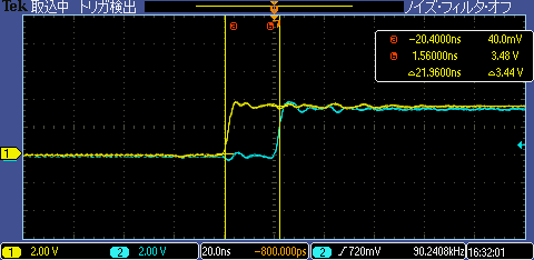
In Technical Reference Manual, it is mentioned “when high-resolution period mode is enabled,
an EPWMxSYNC pulse will introduce +/- 1 - 2 cycle jitter to the PWM. For this reason,
EPWMxSYNCO source should not be set to CTR = 0 or CTR = CMPB. Otherwise, the jitter will occur on every PWM cycle with the synchronization pulse.”
According to this explanation, could you answer me the following questions?
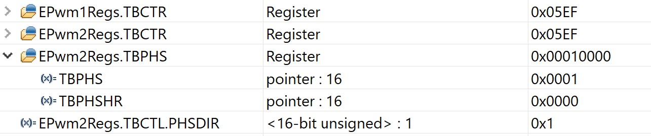
1) Is there a method to avoid the jitter? if it is needed to set EPWMxSYNCO source to CTR = 0 for updating a parameter every PWM cycle in my experiment,
2) If high-resolution period mode is disabled, will the jitter occur when EPWMxSYNCO is set to CTR = 0.
Thank you.
Best regards,
Wenjing