Part Number: LAUNCHXL-F280049C
SPRUI33D – NOVEMBER 2015 – REVISED SEPTEMBER 2020
13.2.1 Clock Configuration
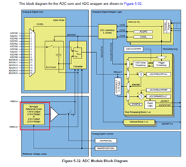
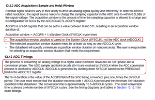
The base ADC clock is provided directly by the system clock (SYSCLK). "This clock is" used to generate the ADC acquisition window. The register ADCCTL2 has a PRESCALE field that determines the ADCCLK. The ADCCLK is used to clock the converter. The core requires approximately 10.5 ADCCLK cycles to process a voltage into a conversion result.
It is necessary for the user to determine the required duration of the acquisition window, see Section 13.13.2.
Given the reference of the ADC clock, "This clock is" to me infers the ADC clock, not the derived from source SYSCLK. The 13.2.1 statement is vague misleading one to believe SYSCLK was the acquisition source clock rate and EOC interrupt pulse source. TRM omitting any kind of peripheral main clock tree or any clock source identification ADC block Fig.13-1 is mind numbing. Adding clock sources in block figures will remove any such question of who is the real clock source. The words "fore mentioned or latter" would infer SYSCLK generates the acquisition window.
Yet 50Mhz ADC sample acquisition rate is not slow by any means and should produce well over 2.5MSPS, upward 3MSPS. The AD converter clocks at SYSCLK speed in other TI family ADC peripherals so the digital FIFO data timing aligns with CPU system BUS timing.