This thread has been locked.

If you have a related question, please click the "Ask a related question" button in the top right corner. The newly created question will be automatically linked to this question.

TMS320F28377D: TMS320F28377D: PCMC

Part Number: TMS320F28377D

My customer encountered the following problems when using DSP (28377d) as synchronous buck or synchronous boost converter and adopting peak current control (PCMC). Please help to solve them. Thank you!

Problem 1: cmps3 is used as the peak current comparison signal, and the external circuit adds a bias value of 1.5V, which is 1.5V when there is no current. By epwm_ Xbar configures the ctriph signal of cmpss3 as trip4, which is input into the DC module of epwm1 to trigger the PWM off signal. See the attachment for the program code.

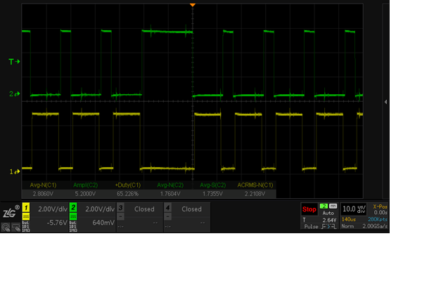
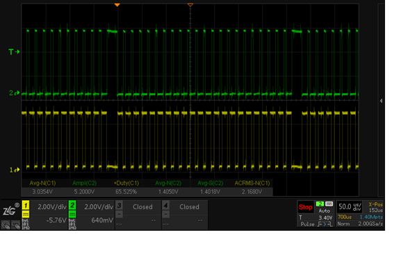
In the experiment, I observed that a wide pulse will be output from time to time, as shown in Figure 1-3 below. In the oscilloscope, CH2 is the synchronous buck main switch and ch1 is the complementary switch
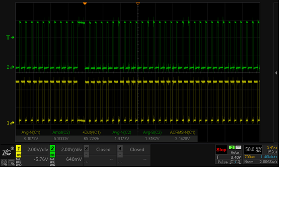
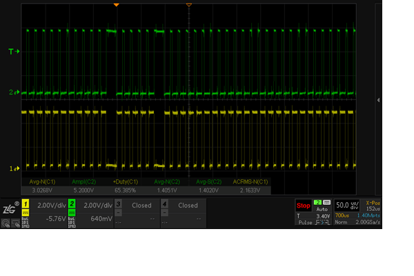
Figure 1

Figure 2

Figure 3

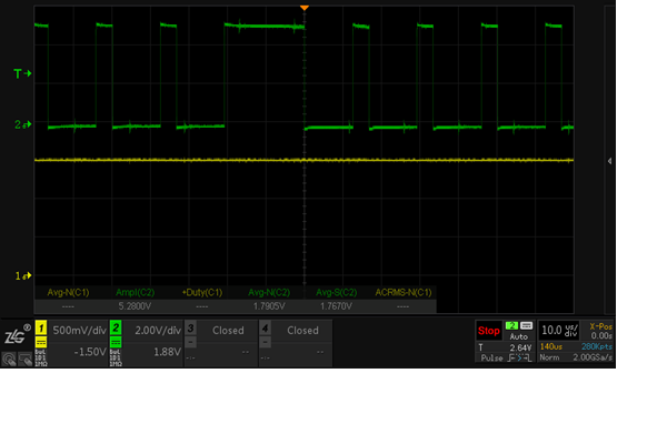
At the same time, my customer also measures the ctripouth signal of cmps3 (output as output3 through configuration), as shown in Figure 5-6. In the oscilloscope, CH2 is the synchronous buck main switch, and ch1 is the ctripouth signal.

Figure 5

Figure 6

My client also measures the cmpin3p signal of cmps3, as shown in ch1 in Figure 7. No interference signal was observed

Figure 7

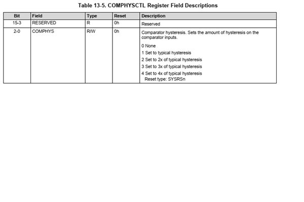
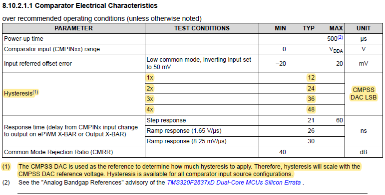
What does typical hypertension mean? Is there any scope?

Is 2x of typical hysteris the above range multiplied by 2?

  • In the experiment, I observed that a wide pulse will be output from time to time, as shown in Figure 1-3 below. In the oscilloscope, CH2 is the synchronous buck main switch and ch1 is the complementary switch
    This sounds similar to the undesired behavior from CMPSS boundary condition issues described in the Errata (search for "CMPSS:") and TRM (search for "CMPSS to Trip").

    At the same time, my customer also measures the ctripouth signal of cmps3 (output as output3 through configuration), as shown in Figure 5-6. In the oscilloscope, CH2 is the synchronous buck main switch, and ch1 is the ctripouth signal.
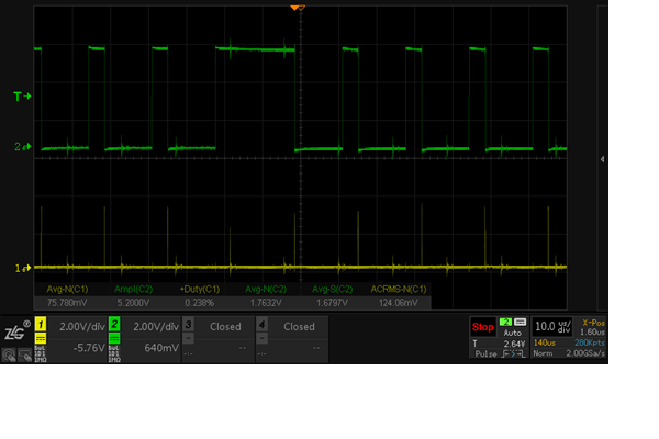
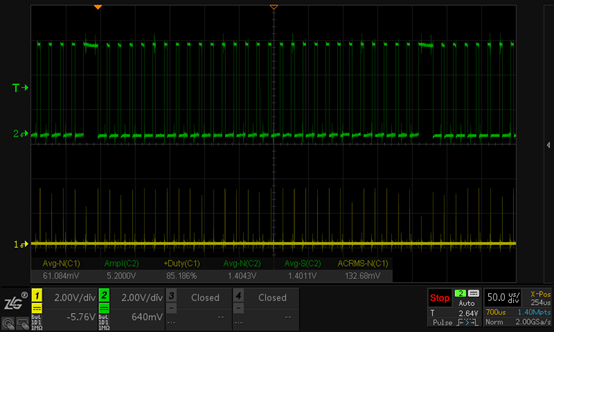
    Which COMPCTL[CTRIPHSEL] selection is your customer using?  For debug, a good starting point is to use the same selection for CTRIPOUTHSEL.  The ASYNCH selection can be useful for observing the comparator response directly without the effects of the digital logic.

    What does typical hypertension mean? Is there any scope?

    Is 2x of typical hysteris the above range multiplied by 2?

    This is described in the datasheet:

  • :thanks for reply.  

        I see the undesired behavior from CMPSS boundary condition issues described in the Errata (search for "CMPSS:") and TRM (search for "CMPSS to Trip"), this behavior may lost a pulse, but my experiment is different,the PWM should be trip by CMPSS,but it keep high untill next cycle.   

       this is the code, can you give me some help,thanks

    /****************************************************************************
    //
    // 文件名:     Main_Buck_Boost_PCMC_V100_CPU1.c
    //
    // 著作权:     Copyright (c) 2020-2025 
    //
    //###########################################################################
    //
    // 创建人员:    Kelvin Li
    //
    // 创建日期:    2021.05.18
    //
    //###########################################################################
    //
    // 内容:  Buck_Boost_CPU1的main函数
    //
    // 描述:  峰值电流控制
    //
    //###########################################################################
    //
    // 修改记录:
    //
    // 版本            | 修改日期                    | 修改人                      | 描述
    // ===== |============|===========|===============================================
    // V1.0  | 2021.05.18 | Kelvin Li | 初始创建版本
    //       |            |           |
    //       |            |           |
    ****************************************************************************/
    
    // Included Files
    #include "F28x_Project.h"
    
    
    //
    // Defines
    //
    //definitions for selecting DACH reference
    #define REFERENCE_VDDA     0
    #define REFERENCE_VDAC     1
    //definitions for COMPH input selection
    #define NEGIN_DAC          0
    #define NEGIN_PIN          1
    //definitions for CTRIPH/CTRIPOUTH output selection
    #define CTRIP_ASYNCH       0
    #define CTRIP_SYNCH        1
    #define CTRIP_FILTER       2
    #define CTRIP_LATCH        3
    
    
    //
    // Function Prototypes
    //
    void InitCMPSS(void);
    void InitEPWM(void);
    
    
    //
    // Main
    //
    void main(void)
    {
        //
        // Step 1. Initialize System Control:
        // PLL, WatchDog, enable Peripheral Clocks
        // This example function is found in the F2837xD_SysCtrl.c file.
        //
            InitSysCtrl();
    
        //
        // Step 2. Initialize GPIO:
        // This example function is found in the F2837xD_Gpio.c file and
        // illustrates how to set the GPIO to it's default state.
        //
            InitGpio();
    
        //
        // Step 3. Clear all interrupts and initialize PIE vector table:
        // Disable CPU interrupts
        //
            DINT;
    
        //
        // Initialize the PIE control registers to their default state.
        // The default state is all PIE interrupts disabled and flags
        // are cleared.
        // This function is found in the F2837xD_PieCtrl.c file.
        //
            InitPieCtrl();
    
        //
        // Disable CPU interrupts and clear all CPU interrupt flags:
        //
            IER = 0x0000;
            IFR = 0x0000;
    
        //
        // Configure Comparator COMP3H to accept POS input from pin and NEG input
        // from DAC
        //
            InitCMPSS();
    
        //
        // Configure GPIO5() to output  OUTPUTXBAR3
        //
            GPIO_SetupPinMux(5, GPIO_MUX_CPU1, 3);
    
        //
        // Configure COMP3 to feed TRIP4 EPWM DC trip input
        //
            InitEPWM();
    
            InitEPwm1Gpio();
    
    
           // Enable PWM
           GPIO_SetupPinMux(4, GPIO_MUX_CPU1, 0);                     // PWMEn1
           GPIO_SetupPinOptions(4, GPIO_OUTPUT, (GPIO_OPENDRAIN | GPIO_PULLUP));       // the standard digital output
           GpioDataRegs.GPACLEAR.bit.GPIO4 = 1;
    
           // Enable PWM
           GPIO_SetupPinMux(10, GPIO_MUX_CPU1, 0);                     // PWMEn2
           GPIO_SetupPinOptions(10, GPIO_OUTPUT, (GPIO_OPENDRAIN | GPIO_PULLUP));       // the standard digital output
           GpioDataRegs.GPACLEAR.bit.GPIO10 = 1;
    
         while(1)
         {
    
         }
    
    }
    
    
    //
    // InitCMPSS - Initialize CMPSS3 and configure settings
    //
    void InitCMPSS(void)
    {
        EALLOW;
    
        //
        //Enable CMPSS
        //
        Cmpss3Regs.COMPCTL.bit.COMPDACE = 1;
    
        //
        //NEG signal comes from DAC
        //
        Cmpss3Regs.COMPCTL.bit.COMPHSOURCE = NEGIN_DAC;
    
        //
        //Use VDDA as the reference for DAC
        //
        Cmpss3Regs.COMPDACCTL.bit.SELREF = REFERENCE_VDDA;
    
        //
        // Configure CTRIPOUT path
        // Asynch output feeds CTRIPH and CTRIPOUTH
        //
        Cmpss3Regs.COMPCTL.bit.CTRIPHSEL = CTRIP_ASYNCH;
        Cmpss3Regs.COMPCTL.bit.CTRIPOUTHSEL = CTRIP_ASYNCH;
    
        //
        // Configure CTRIPOUTH output pin
        // Configure OUTPUTXBAR3 to be CTRIPOUT1H
        //
        OutputXbarRegs.OUTPUT3MUX0TO15CFG.bit.MUX4 = 0;
    
        //
        //Enable OUTPUTXBAR3 Mux for Output
        //
        OutputXbarRegs.OUTPUT3MUXENABLE.bit.MUX4 = 1;


        //
        //DAC source select. Determines whether DACHVALA is updated from DACHVALS or from the ramp generator
        //
        Cmpss3Regs.COMPDACCTL.bit.DACSOURCE = 1;       // 0 DAC updated from DACHVALS, 1 DAC updated from the ramp generator
    
        //
        //Ramp generator source select. Determines which EPWMSYNCPER signal is used within the CMPSS module
        //
        Cmpss3Regs.COMPDACCTL.bit.RAMPSOURCE = 0;       // 0 EPWM1SYNCPER, 3 EPWM4SYNCPER
    
        EDIS;
    
    
        Cmpss3Regs.RAMPDECVALS = 5;
    
        Cmpss3Regs.RAMPMAXREFS = 35000;
    }
    
    
    //
    // InitEPWM - Initialize EPWM1 module settings
    //
    void InitEPWM(void)
    {
        EALLOW;
        CpuSysRegs.PCLKCR0.bit.TBCLKSYNC = 0;
    
        //
        //Configure EPWM to run at SYSCLK
        //
    //    ClkCfgRegs.PERCLKDIVSEL.bit.EPWMCLKDIV = 0;
        EPwm1Regs.TBCTL.bit.CLKDIV = 0;
        EPwm1Regs.TBCTL.bit.HSPCLKDIV = 0;
    
        //
        //Initialize dummy values for EPWM CTR/PRD
        //
        EPwm1Regs.TBCTR = 0;
        EPwm1Regs.TBPRD = 1667;         // 60kHz PWM
    
        CpuSysRegs.PCLKCR0.bit.TBCLKSYNC = 1;
    
        //
        //Configure TRIP4 to be CTRIP3H
        //
        EPwmXbarRegs.TRIP4MUX0TO15CFG.bit.MUX4 = 0;
    
        //
        //Enable TRIP4 Mux for Output
        //
        EPwmXbarRegs.TRIP4MUXENABLE.bit.MUX4 = 1;
    
        //
        // Enable PWM
        //
        EPwm1Regs.TBCTL.bit.CTRMODE = TB_COUNT_UP;
    
        //
        // Set actions
        //
        EPwm1Regs.AQCTLA.bit.ZRO = AQ_SET;      // Set PWM1A on event A, up count
    //    EPwm1Regs.AQCTLA.bit.CAU = AQ_CLEAR;    // Clear PWM1A on event A, down count
        EPwm1Regs.AQCTLA2.bit.T2U = AQ_CLEAR;   // Action when event occurs on T2 in UP-Count
    
    //    EPwm1Regs.AQCTLB.bit.ZRO = AQ_SET;      // Set PWM1B on event B, up count
    //    EPwm1Regs.AQCTLB.bit.CAU = AQ_CLEAR;      // Set PWM1B on event B, up count
    //    EPwm1Regs.AQCTLB2.bit.T2U = AQ_CLEAR;   // Action when event occurs on T2 in UP-Count
    
        EPwm1Regs.AQTSRCSEL.bit.T2SEL = 1;      // 0:DCAEVT1, 1:DCAEVT2, 2:DCBEVT1, 3:DCBEVT2
        //
        // Active Low PWMs - Setup Deadband
        //
    //    EPwm1Regs.DBCTL.bit.HALFCYCLE = 1;     // Half cycle clocking enabled
        EPwm1Regs.DBCTL.bit.OUT_MODE = DB_FULL_ENABLE;
        EPwm1Regs.DBCTL.bit.POLSEL = DB_ACTV_HIC;
        EPwm1Regs.DBCTL.bit.IN_MODE = DBA_ALL;
        EPwm1Regs.DBRED.bit.DBRED = 80;
        EPwm1Regs.DBFED.bit.DBFED = 80;
    
    //    EPwm1Regs.TZSEL.bit.DCAEVT2 = 1;            // Enable DCAEVT2 as a CBC trip source for this ePWM module
    
    //    EPwm1Regs.TZCTL.bit.DCAEVT2 = TZ_FORCE_LO;  // 10: Force EPWMxA to a low state
    //    EPwm1Regs.TZCTL.bit.DCBEVT2 = TZ_NO_CHANGE;  // 11: Do Nothing, trip action is disabled
    
    
        EPwm1Regs.DCTRIPSEL.bit.DCAHCOMPSEL = 3;       // Trip 4
    //    EPwm1Regs.DCTRIPSEL.bit.DCBHCOMPSEL = 3;    // Trip 4
    
        EPwm1Regs.TZDCSEL.bit.DCAEVT2 = TZ_DCAH_HI;    // 010: DCAH = high, DCAL = don't care
    //    EPwm1Regs.TZDCSEL.bit.DCBEVT2 = 2;          // 010: DCBH = high, DCBL = don't care
    
    //    EPwm1Regs.DCACTL.bit.EVT2SRCSEL = 0;        // 0: Source Is DCAEVT1 Signal;  1: Source Is DCEVTFILT Signal
    //    EPwm1Regs.DCACTL.bit.EVT2FRCSYNCSEL = 1;    // 0: Source is synchronized with EPWMCLK;   1: Source is passed through asynchronously
    
        EPwm1Regs.DCFCTL.bit.SRCSEL = 1;            // 01: Source Is DCAEVT2 Signal
        EPwm1Regs.DCFCTL.bit.BLANKE = 1;            // 1: Blanking window is enabled
        EPwm1Regs.DCFCTL.bit.BLANKINV = 0;          // 0: Blanking window not inverted;  1: Blanking window inverted
        EPwm1Regs.DCFCTL.bit.PULSESEL = 1;          // 01: Time-base counter equal to zero
    
        EPwm1Regs.HRPCTL.bit.PWMSYNCSELX = 0;         // EPWMSYNCPER is defined by PWMSYNCSEL
        EPwm1Regs.HRPCTL.bit.PWMSYNCSEL = 1;          // 1:CTR = zero;  0:CTR = PRD
    
        EDIS;
    
        EPwm1Regs.DCFOFFSET = 0;
        EPwm1Regs.DCFWINDOW = 106;
    }
    
    /****************************************************************************
    // No more.
    ****************************************************************************/


  • this behavior may lost a pulse, but my experiment is different,the PWM should be trip by CMPSS,but it keep high untill next cycle. 

    This is helpful clarification. The scope pictures are a bit small for full context.

    It may still be a boundary-condition scenario. It looks like a synchronization problem between the comparator and EPWM when it comes to conveying the trip status.

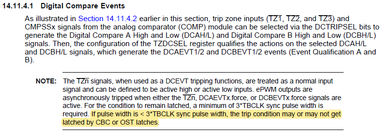
    There is a note in the Digital Compare section of the TRM that calls for the DC input trip signals to be asserted for at least three EPWM TBCLK cycles:

    The code snippet appears to be selecting the ASYNC comparator signal as the EPWM trip source. The ASYNC signal is not guaranteed to satisfy the 3*TBCLK cycle requirement by itself.  The digital filter (COMPHSTS) or latched (COMPHLATCH) signals would be better suited for satisfying the 3*TBCLK cycle requirement.

    It is possible that for some PWM cycles, the Ramp Generator may be qualifying a local trip and resetting the RAMPSTS value to RAMPMAXREF before the ASYNC trip signal satisfies the 3*TBCLK cycle requirement of the EPWM.

    In the scope capture of the comparator input, it looks like a DC test signal is being used to test the CMPSS behavior. For a DC test input, the DACVAL will be held static above the input voltage until the Ramp Generator is released to decrement on the next PWMSYNCPER signal.

    For a real system where the input represents the plant feedback, the comparator would most likely trip the EPWM after some delay when the feedback eventually exceeds RAMPMAXREF for 3*TBCLK cycles.

  • The digital filter (COMPHSTS) or latched (COMPHLATCH) signals would be better suited for satisfying the 3*TBCLK cycle requirement

    I use digital filter (COMPHSTS) signal  to trip the PWM,  the PWM work well.  

    Thank you for solving problems.