This thread has been locked.

If you have a related question, please click the "Ask a related question" button in the top right corner. The newly created question will be automatically linked to this question.

TMS320F280025-Q1: ADC transform mode

Part Number: TMS320F280025-Q1

Hi

ADC conversion, wish to set to continuous conversion mode, and sent to DMA,

The first time I start the conversion, the next time I don't have to do it, just go straight to the DMA memory read line.

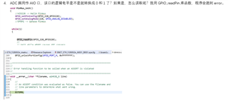
However, when I look at the routine and see the user manual (as below Figure 1), the ADC continuous conversion is interrupted by the completion of the conversion.

Interrupt and then start the next conversion to achieve continuous conversion, not what I expected, but what I expected was that the software would start the transformation first, then the ADC transformation would finish and then start the transformation itself, and so on.please help to confirm this.

F28335 is set by ADC's conversion mode, such as single conversion mode and cyclic scanning mode, etc. I don't seem to see the relevant register bits for F280025 to set, please help to confirm this.

Thanks!

  • Hi Neal,

    The "continue to interrupt" bit only allows the ISR pulse to propagate to the ePIE or DMA without the CPU explicitly clearing the ISR bit.  It does not otherwise control the triggering or sequence of which channels are converted: the pulses to the ePIE or DMA therefore won't continue unless some other mechanism is used to trigger conversions.

    Usually an ePWM module would be the source that would continue to trigger conversions (by triggering SOCs periodically) but it is also possible to setup the ADC INT flag itself to be the trigger source for SOCs.  In this case, you can either have an SOC trigger itself to get continuous conversions (e.g. SOC0 triggers ADCINT1 and ADCINT1 triggers SOC0 and a SW trigger starts the process) or you can setup "ping-pong" sampling.  In it's simplest form, ping pong sampling works e.g. SOC0 to SOC7 are triggered by ADCINT2, SOC8 to SOC16 are triggered by ADCINT1.  SOC7 triggers ADCINT1 and SOC15 triggers ADCINT2.  SW starts the process by triggering SOC0 to SOC7.  The advantage of this is that RESULT0 to 7 can be read while SOC8 to SOC15 convert and vice-versa for RESULT8 to 15 while SOC0 to SOC7 converts.      

  • Hi

    ADC pin is used as AIO port. Is the logic level of the port converted to 0 and 1?
    If so, how to read it? I use GPIO_ Readpin library function, the program will run to error.

    Thanks!

  • Hi Neal,

    The AIOs should function like a normal GPIO for reading (note that they are input only, so you can't write to them or put them in output mode).  For instance, if you are using AIO231, the interface should be through GPIO231.  

    Can you provide more detail on the error you are seeing?

    (Also note that in the future it is generally better to create a new thread if you have a new unrelated question: use the "Ask a new question" button)

  • Hi

    FYI,thanks!

  • Hi Neal,

    The only assertion in GPIO_readPin() is GPIO_isPinValid(pin).  This checks that pin is between

    return((pin <= 59U) || ((pin >= 224U) && (pin <= 247U)));

    So the value 228 should be OK.  

    What is the value of the #define GPIO_228_GPIO228?  Is this user defined?