This thread has been locked.

If you have a related question, please click the "Ask a related question" button in the top right corner. The newly created question will be automatically linked to this question.

TMDSPREX28335: TMDSPREX28335: GPIO TOGGLE erratic behaviour

Part Number: TMDSPREX28335
Other Parts Discussed in Thread: CONTROLSUITE

Hello Everyone,

I have a TMDSPREX28335 experimental kit with me. It has got 4 LEDs on it and they are connected to the GPIOs as follows:

LED1: GPIO9

LED2: GPIO11

LED3: GPIO34

LED4: GPIO49

In order to understand the kit I used the concept of the Example_2833xGpioToggle.c program and modified it to only toggle the 4 LEDs and the corresponding GPIOs. The code is attached for clarity.

// OBJECTIVE IS TO CONFIGURE GPIOs AS GPIOs
// AND TOGGLE TO OBTAIN A PWM OUTPUT ON OSCILLOSCOPE
// using TOGGLE registers to TOGGLE
// Included Files
//
#include "DSP28x_Project.h"     // Device Headerfile and Examples Include File

//
// Defines that select the example to compile in.
// Only one example should be set as 1 the rest should be set as 0.
//
#define EXAMPLE3 1  // Use TOGGLE registers to toggle I/O's

//
// Function Prototypes
//
void delay_loop(void);
void Gpio_example3(void);

//
// Main
//
void main(void)
{
    //
    // Step 1. Initialize System Control:
    // PLL, WatchDog, enable Peripheral Clocks
    // This example function is found in the DSP2833x_SysCtrl.c file.
    //
    InitSysCtrl();

    //
    // Step 2. Initialize GPIO:
    // This example function is found in the DSP2833x_Gpio.c file and
    // illustrates how to set the GPIO to it's default state.
    //
    // InitGpio();  // Skipped for this example

    //
    // For this example use the following configuration
    //
    EALLOW;
    GpioCtrlRegs.GPAMUX1.all = 0x00000000;  // All GPIO
    GpioCtrlRegs.GPAMUX2.all = 0x00000000;  // All GPIO
    GpioCtrlRegs.GPBMUX1.all = 0x00000000;  // All GPIO
    GpioCtrlRegs.GPBMUX2.all = 0x00000000;  // All GPIO
    GpioCtrlRegs.GPADIR.all = 0xFFFFFFFF;   // All outputs
    GpioCtrlRegs.GPBDIR.all = 0xFFFFFFFF;   // All outputs
    GpioCtrlRegs.GPAQSEL1.all = 0x0000;    // GPIO0-GPIO15 Synch to SYSCLKOUT
    GpioCtrlRegs.GPAQSEL2.all = 0x0000;    // GPIO16-GPIO31 Synch to SYSCLKOUT
    GpioCtrlRegs.GPBQSEL1.all = 0x0000;    // GPIO32-GPIO39 Synch to SYSCLKOUT
    GpioCtrlRegs.GPBQSEL2.all = 0x0000;    // GPIO48-GPIO63 Synch to SYSCLKOUT
    GpioCtrlRegs.GPAPUD.all = 0xFFFFFFFF;    // Pullup's disabled GPIO0-GPIO31
    GpioCtrlRegs.GPBPUD.all = 0xFFFFFFFF;    // Pullup's disabled GPIO32-GPIO34
    EDIS;
    //
    // Step 3. Clear all interrupts and initialize PIE vector table
    // Disable CPU interrupts
    //
    DINT;

    //
    // Initialize PIE control registers to their default state.
    // The default state is all PIE interrupts disabled and flags
    // are cleared.
    // This function is found in the DSP2833x_PieCtrl.c file.
    //
    InitPieCtrl();

    //
    // Disable CPU interrupts and clear all CPU interrupt flags
    //
    IER = 0x0000;
    IFR = 0x0000;

    //
    // Initialize the PIE vector table with pointers to the shell Interrupt
    // Service Routines (ISR).
    // This will populate the entire table, even if the interrupt
    // is not used in this example.  This is useful for debug purposes.
    // The shell ISR routines are found in DSP2833x_DefaultIsr.c.
    // This function is found in DSP2833x_PieVect.c.
    //
    InitPieVectTable();

    //
    // Step 4. Initialize all the Device Peripherals:
    // This function is found in DSP2833x_InitPeripherals.c
    //
    // InitPeripherals(); // Not required for this example

    //
    // Step 5. User specific code:
    //
#if EXAMPLE3
    //
    // This example uses TOGGLE registers to toggle I/O's
    //
    Gpio_example3();
#endif
}

//
// delay_loop -
//
void delay_loop()
{
    volatile long i;
    for (i = 0; i < 5000000; i++)
    {
        asm(" NOP");
        EALLOW;
        SysCtrlRegs.WDKEY = 0x55;
        SysCtrlRegs.WDKEY = 0xAA;
        EDIS;
    }
}

//
// Gpio_example3 -
//
void Gpio_example3(void)
{
    //
    // Example 2: Toggle I/Os using TOGGLE registers
    //

    //
    // Set pins to a known state
    //
    GpioDataRegs.GPADAT.bit.GPIO9 =1;
    GpioDataRegs.GPADAT.bit.GPIO11 =0;
    GpioDataRegs.GPBDAT.bit.GPIO34 =1;
    GpioDataRegs.GPBDAT.bit.GPIO49 =0;
    //
    // Use TOGGLE registers to flip the state of the pins.
    // Any bit set to a 1 will flip state (toggle)
    // Any bit set to a 0 will not toggle.
    //
    for(;;)
    {
        GpioDataRegs.GPATOGGLE.bit.GPIO9 =1;
        GpioDataRegs.GPATOGGLE.bit.GPIO11 =1;
        GpioDataRegs.GPBTOGGLE.bit.GPIO34 =1;
        GpioDataRegs.GPBTOGGLE.bit.GPIO49 =1;
        delay_loop();
    }
}

//
// End of File
//

If I modify the code a bit from line 131 to line 134 as per the details in the attached table I see an unexpected sort of a behaviour from the kit. The observations are also included in the table.

Case 1 Case 2 Case 3 Case 4 Case 5 Case 6 Case 7
GPIO (LED) GPxDAT GPxDAT GPxSET GPxSET GPxSET GPxCLEAR GPxCLEAR
9 (1) 1 0 0 1 0 1 0
11 (2) 0 1 0 0 1 0 1
34 (3) 1 0 1 1 0 1 0
49 (4) 0 1 1 0 1 0 1
Observations LED1 and LED2 should switch complementary to each other
however, they both switch ON and OFF at the same time.
LED3 and LED4 are switching complementary to each other.

Erratic behaviour
LED1 and LED2 are glowing alternatively.
LED3 and LED4 are glowing alternatively.


Normal behaviour

LED1 and LED2 are not glowing at all. LED3 and LED4 are glowing at the same.

Erratic behaviour

LED1 and LED2 are glowing alternatively.
LED3 and LED4 are glowing alternatively.


Normal behaviour
LED1 and LED2 are glowing alternatively.
LED3 and LED4 are glowing alternatively.


Normal behaviour
LED1, LED2, LED3, and LED4 all are switching ON and OFF at the same time.


Erratic behaviour
LED1, LED2, LED3, and LED4 all are switching ON and OFF at the same time.


Erratic behaviour

Can anyone throw some light on why  I am encountering such exceptional behaviour in cases 1, 3, 6 and 7?

With Regards,

Ankit

PS: There might be many more possible combinations that I haven't tried which may possibly generate unexpected outputs!!!!!

PPS: A thorough explanation or/and criticism is/are more than welcome Slight smileMoney mouth

  • Ankit,

    Thanks for reaching out to the E2E Forum.  I don't see anything incorrect in your code, I'm trying to locate a PREX board locally to see if I can reproduce.

    In the meantime can you find jumpers J8 and J9 and make sure they are not populated?  The intent of the jumpers is to tie LED1 and LED2 to the SPI channels to show activity, but in this case the GPIOs for those signals could be driving against any "1" you write to GPIO9 and GPIO11 assuming the default config.

    Best,
    Matthew

  • Hello Matthew,

    I am thankful for your generous input and my sincere apologies for not replying immediately.

    I did indeed remove the jumpers J8 and J9 as per your suggestion from the board and to my astonishment, all the possible 16 combinations in the attached table for GPxSET got verified

    Gpio (LED) Case 1 Case 2 Case 3 Case 4 Case 5 Case 6 Case 7 Case 8 Case 9 Case 10 Case 11 Case 12 Case 13 Case 14 Case 15 Case 16
    09 (1) 0 0 0 0 0 0 0 0 1 1 1 1 1 1 1 1
    11 (2) 0 0 0 0 1 1 1 1 0 0 0 0 1 1 1 1
    34 (3) 0 0 1 1 0 0 1 1 0 0 1 1 0 0 1 1
    49 (4) 0 1 0 1 0 1 0 1 0 1 0 1 0 1 0 1

    However, all these 16 combinations did not give the expected outputs for both GPxCLEAR and GPxDAT on TOGGLE.

    CLEAR = 0 and DAT = 1 should make (as per my understanding and I can definitely be horribly wrong) the GPIO as HIGH. Similarly, CLEAR = 1 and DAT = 0 should make the GPIO LOW.

    So if we toggle CLEAR = 0; DAT = 1  (GPIO = HIGH) we should get CLEAR = 1; DAT = 0 (GPIO = LOW). Then why is TOGGLE giving an unexpected output?

    Could it be that I am making an incorrect assumption?

    I would appreciate it if you can clarify this concept for me Slight smile.

    With Regards,

    Ankit

  • Ankit,

    I'm glad the jumpers were the cause of the external drive issue.

    In terms of the GPIOTOGGLE/GPIOCLEAR/GPIOSET registers, these will always read back "0".  While writing a "1" to them will have the effect you have mentioned on the respective GPIO pin, there is no information in the register to read back to determine the state of the GPIO pin or if the register bit was previously set.

    Only the GPIODAT register will show the current state of the GPIO pin; in addition it can also be written to effect the state of the GPIO pin.

    We include the TOGGLE/SET/CLEAR as it provides a less intrusive way to change the GPIO pin state, as well as saving any read back cycles for the C28x CPU, vs using the GPIODAT register to change the pin state.

    Best,

    Matthew

  • Hello Matthew,

    I am again thankful for your inputs and I must apologize again for such a late reply due to health issues.
    I understand that it is difficult to predict what output one might get on TOGGLING GPIOCLEAR=0 and thus it may preferably be avoided.
    However, I experienced no such dilemma when it was about TOGGLING GPIOSET=0.

    Another statement that I would like to make here is about the GPxDAT register.

    GPIO
    (LED)
    Case
    1
    Case
    2
    Case
    3
    Case
    4
    Case
    5
    Case
    6
    Case
    7
    Case
    8
    Case
    9
    Case
    10
    Case
    11
    Case
    12
    Case
    13
    Case
    14
    Case
    15
    Case
    16
    09 (1) 0 0 0 0 0 0 0 0 1 1 1 1 1 1 1 1
    11 (2) 0 0 0 0 1 1 1 1 0 0 0 0 1 1 1 1
    34 (3) 0 0 1 1 0 0 1 1 0 0 1 1 0 0 1 1
    49 (4) 0 1 0 1 0 1 0 1 0 1 0 1 0 1 0 1
    Observation Normal behaviour Normal behaviour Normal behaviour Normal behaviour Normal behaviour Normal behaviour Normal behaviour Normal behaviour GPIOs 11, 34 and 49 should switch together and be complementary to GPIO 9.
    However, all the GPIOs are switching ON and OFF at the same time. 
    GPIOs 9 and 49 should switch together and be complementary to GPIOs 11 and 34.
    However, GPIOs 9, 11 and 34 are switching ON and OFF at the same time while being complementary to the GPIO 49.
    GPIOs 9 and 34 should be high at the same time and complementary to GPIOs 11 and 49.
    Whereas, GPIOs 9, 11 and 49 show the same output and it is complementary to GPIO 34.
    GPIOs 9, 34 and 49 should be in phase and GPIO 11 should be out of phase. But this time 9 and 11 work together but in opposition to 34 and 49. GPIOs 9 and 11 should be high together and 34 and 49 should be low together.
    This time GPIOs 9, 34 and 49 are in phase and GPIO 11 is out of phase.
    GPIOs 9, 11 and 49 should be complementary to GPIO 34 however, during the test GPIOs 9 and 34 are in phase with each other while being out of phase with GPIOs 11 and 49 at the same time. GPIOs 9, 11 and 34 should be HIGH at the same time while GPIO 49 should be low.
    This time GPIOs 9 and 49 are in phase with each other while being complementary to GPIOs 11 and 34.
    All the GPIOs should toggle together, however, GPIO 9 is out of phase with GPIOs 11, 34 and 49.

    The only thing that I am able to concur from the above table is that the TOGGLING action is working fine GPxDAT register till the time the 9th GPIO is 0.
    As soon as I make GPIO 9 as 1 it starts to toggle the other three GPIOs 11, 34 and 49.
    From your last response, I am making an assumption that it is okay to TOGGLE while using the GPxDAT register, but I have been proved wrong already.
    And as of now, I have only played with the 4 LEDs so far. Could it be that by making GPxDAT = 1 into GPIO 09 can force the output of other GPIOs to toggle forcefully?
    Am I making a mistake somewhere?

    With Regards,
    Ankit

    PS: J8 and J9 are still removed from the board

  • Ankit,

    GPIO9 should not have any impact on the other GPIOs.  I think this must be HW related on the PREX or the control CARD if you are seeing this behavior.

    While l look at the schematics for any potential explanations, can you perform the following:

    Make the GPADIR/GPBDIR for GPIOs 11, 34, 49 all 0; that is making them inputs only.

    Keep GPIO 9 as output(with GPADIR =1) and change its state using the GPADAT register; do you still observe the other IOs following GPIO9?

    If so do you see the GPxDAT associated with each IO reflecting the state of the pin?

    Can you also attach the code for going through the above states(if it is different than the one posted before).

    Hope you are feeling better as well.

    Best,

    Matthew

  • Hello Matthew,

    Yeah, all well now!! And again thanks for the prompt reply.

    I did what you told me to. I locked GPIOs 11, 34, and 49 to behave as input by making their DIRs 0 while keeping GPIO 9 as output. I tried all the 16 possible combinations of 1s and 0s on GPxDAT with GPIOs 9, 11, 34, and 49 and TOGGLED all of these cases. As expected only GPIO 9 exhibited the toggling behaviour. However, there was one more observation from all of these 16 iterations. GPIO 34 (LED 3) remained permanently OFF and GPIOs 11, 49 (LEDs 2, 4) remained permanently ON.

    Either all of them (11, 34, and 49) should be high together or low together because these are acting as INPUTS but why 34 is complementary to both 11 and 49?

    Are we opening a can of worms here by going too deep into seeking clarifications?

    With Regards,
    Ankit

  • Ankit,

    No worries, the GPIO logic should operate in a straightforward fashion, and for some reason it is not.  As I mentioned before there's nothing that should cause this from a device POV, so I think there is some gotchas lurking on the PREX board that we are both not catching.

    I think GPIO49 may be the result of the internal pull up on this pin.  GPIO34 should have this as well from reset, while GPIO11 is disabled.

    If you can check the GPAPUD and GPBPUD registers, if will confirm which are disabled(1 is disabled).  Perhaps the code we are running has set these differently than reset.

    I'll try to manually check this on my PREX board tomm in any case.

    Best,

    Matthew

  • Hello Matthew,

    Again thanks for your input and your assurance means a lot during this debugging phase.

    PUD is 1 on all GPIOs (lines 53 and 54 of the code).

    I hope this helps.

    With regards,
    Ankit

  • Ankit,

    I'll need another day to get the data, appreciate your patience here.

    Best,

    Matthew

  • Hey Matthew,

    No worries at all. Please take your time.

    With Regards,
    Ankit

    PS: Terribly sorry for being such a pain in the neck to you!!

  • Hello Matthew,

    I shall apologise in advance as this is going to bring in more trouble for you from myside.

    For some reason, I am unable to ask a new question and that is why I shall try to reply to this post and ask my queries.

    Query 1: Why is it so that I am being taken to the following URL (https://e2e.ti.com/p/ti_errorpage) every time I try to ask a new question?

    Query 2: Can you help me with the DBRED, TBCLK, and TBPRD calculations?

    I have the following settings:
    FSYSCLKOUT = 150 MHz which means TSYSCLKOUT = 6.6667 ns = SYSCLKOUT
    CLKDIV = 0 i.e., CLKDIV = 1
    HSPCLKDIV = 1 i.e., HSPCLKDIV = 2

    I need to create a rising edge delay of 10 µs. And I need a PWM of 1 kHz or TPWM = 1 ms.

    TBCLK Calculation:

    TBCLK = SYSCLKOUT/(HSPCLKDIV*CLKDIV)
    TBCLK = (6.6667 ns)/(2*1)
    TBCLK = 3.33335 ns
    TBPRD Calculation (for UP-DOWN mode):

    TBPRD = 0.5*TPWM/(TSYSCLKOUT*HSPCLKDIV*CLKDIV)
    TBPRD = 0.5*(1 ms)/(6.6667 ns*2*1)
    TBPRD = 37500

    DBRED Calculation:

    Rising Edge Delay = TBCLK*DBRED
    DBRED = Rising Edge Delay/TBCLK
    DBRED = (10 µs)/(3.33335 ns)
    DBRED = 2999.985 ~ 3000


    However as per the following code DBRED = 750 to generate the same time delay of 10 µs (refer lines 132 and 133 of the code).

    //
    //      Lab7_6: TMS320F28335
    //      (c) Frank Bormann
    //
    //###########################################################################
    //
    // FILE:	Lab7_6.c
    // 
    // TITLE:	DSP28335ControlCARD; ePWM1A 1KHz output
    //			variable pulse width
    //			complementary signal at ePWM1B
    //			plus dead band rising edge delay
    //			solution file for Lab7_6
    //###########################################################################
    //  Ver | dd mmm yyyy | Who  | Description of changes
    // =====|=============|======|===============================================
    //  3.0 | 15 Apr 2009 | F.B. | Lab7_6 for F28335; 
    //  3.1 | 10 Nov 2009 | F.B  | Lab7_6 for F28335 and PE revision 5
    //###########################################################################
    #include "DSP2833x_Device.h"
    
    // external function prototypes
    extern void InitSysCtrl(void);
    extern void InitPieCtrl(void);
    extern void InitPieVectTable(void);
    extern void InitCpuTimers(void);
    extern void ConfigCpuTimer(struct CPUTIMER_VARS *, float, float);
    
    
    // Prototype statements for functions found within this file.
    void Gpio_select(void);
    void Setup_ePWM1(void);
    interrupt void cpu_timer0_isr(void);
    
    //###########################################################################
    //						main code									
    //###########################################################################
    void main(void)
    {
    	int counter=0;	// binary counter for digital output
    
    	InitSysCtrl();	// Basic Core Init from DSP2833x_SysCtrl.c
    
    	EALLOW;
       	SysCtrlRegs.WDCR= 0x00AF;	// Re-enable the watchdog 
       	EDIS;			// 0x00AF  to NOT disable the Watchdog, Prescaler = 64
    
    	DINT;				// Disable all interrupts
    	
    	Gpio_select();		// GPIO9, GPIO11, GPIO34 and GPIO49 as output
    					    // to 4 LEDs at Peripheral Explorer Board
    
    	Setup_ePWM1();		// init of ePWM1A
    
    	InitPieCtrl();		// basic setup of PIE table; from DSP2833x_PieCtrl.c
    	
    	InitPieVectTable();	// default ISR's in PIE
    
    	EALLOW;
    	PieVectTable.TINT0 = &cpu_timer0_isr;
    	EDIS;
    
    	InitCpuTimers();	// basic setup CPU Timer0, 1 and 2
    
    	ConfigCpuTimer(&CpuTimer0,150,100);
    
    	PieCtrlRegs.PIEIER1.bit.INTx7 = 1;
    
    	IER |=1;
    
    	EINT;
    	ERTM;
    
    	CpuTimer0Regs.TCR.bit.TSS = 0;	// start timer0
    
    	while(1)
    	{    
    	  		while(CpuTimer0.InterruptCount == 0);
    			CpuTimer0.InterruptCount = 0;
    			
    			EALLOW;
    			SysCtrlRegs.WDKEY = 0x55;	// service WD #1
    			EDIS;
    
    	  		counter++;
    			if(counter&1) GpioDataRegs.GPASET.bit.GPIO9 = 1;
    				else GpioDataRegs.GPACLEAR.bit.GPIO9 = 1;
    			if(counter&2) GpioDataRegs.GPASET.bit.GPIO11 = 1;
    				else GpioDataRegs.GPACLEAR.bit.GPIO11 = 1;
    			if(counter&4) GpioDataRegs.GPBSET.bit.GPIO34 = 1;
    				else GpioDataRegs.GPBCLEAR.bit.GPIO34 = 1;
    			if(counter&8) GpioDataRegs.GPBSET.bit.GPIO49 = 1;
    				else GpioDataRegs.GPBCLEAR.bit.GPIO49 = 1;
    	}
    } 
    
    void Gpio_select(void)
    {
    	EALLOW;
    	GpioCtrlRegs.GPAMUX1.all = 0;		// GPIO15 ... GPIO0 = General Puropse I/O
    	GpioCtrlRegs.GPAMUX1.bit.GPIO0 = 1;	// ePWM1A active
    	GpioCtrlRegs.GPAMUX1.bit.GPIO1 = 1;	// ePWM1B active
    
    	GpioCtrlRegs.GPAMUX2.all = 0;		// GPIO31 ... GPIO16 = General Purpose I/O
    	GpioCtrlRegs.GPBMUX1.all = 0;		// GPIO47 ... GPIO32 = General Purpose I/O
    	GpioCtrlRegs.GPBMUX2.all = 0;		// GPIO63 ... GPIO48 = General Purpose I/O
    	GpioCtrlRegs.GPCMUX1.all = 0;		// GPIO79 ... GPIO64 = General Purpose I/O
    	GpioCtrlRegs.GPCMUX2.all = 0;		// GPIO87 ... GPIO80 = General Purpose I/O
    	 
    	GpioCtrlRegs.GPADIR.all = 0;
    	GpioCtrlRegs.GPADIR.bit.GPIO9 = 1;	// peripheral explorer: LED LD1 at GPIO9
    	GpioCtrlRegs.GPADIR.bit.GPIO11 = 1;	// peripheral explorer: LED LD2 at GPIO11
    
    	GpioCtrlRegs.GPBDIR.all = 0;		// GPIO63-32 as inputs
    	GpioCtrlRegs.GPBDIR.bit.GPIO34 = 1;	// peripheral explorer: LED LD3 at GPIO34
    	GpioCtrlRegs.GPBDIR.bit.GPIO49 = 1; // peripheral explorer: LED LD4 at GPIO49
    	GpioCtrlRegs.GPCDIR.all = 0;		// GPIO87-64 as inputs
    	EDIS;
    }  
    
    void Setup_ePWM1(void)
    {
    	EPwm1Regs.TBCTL.bit.CLKDIV =  0;	// CLKDIV = 1		
    	EPwm1Regs.TBCTL.bit.HSPCLKDIV = 1;	// HSPCLKDIV = 2
    	EPwm1Regs.TBCTL.bit.CTRMODE = 2;	// up - down mode
    
    	EPwm1Regs.AQCTLA.all = 0x0060;		// set ePWM1A on CMPA up
    										// clear ePWM1A on CMPA down
    	EPwm1Regs.TBPRD = 37500;			// 1KHz - PWM signal
    	EPwm1Regs.CMPA.half.CMPA  = 18750;	// 50% duty cycle first
    
    	EPwm1Regs.DBRED = 750;				// 10 microseconds delay
    	EPwm1Regs.DBFED = 750;				// for rising and falling edge
    	EPwm1Regs.DBCTL.bit.OUT_MODE = 3;	// ePWM1A = RED
    	EPwm1Regs.DBCTL.bit.POLSEL = 2;		// S3=1 inverted signal at ePWM1B
    	EPwm1Regs.DBCTL.bit.IN_MODE = 0;	// ePWM1A = source for RED & FED
    } 
    
    interrupt void cpu_timer0_isr(void)
    {
    	
    	CpuTimer0.InterruptCount++;
    	EALLOW;
    	SysCtrlRegs.WDKEY = 0xAA;	// service WD #2
    	EDIS;
    	PieCtrlRegs.PIEACK.all = PIEACK_GROUP1;
    }
    //===========================================================================
    // End of SourceCode.
    //===========================================================================


    Have I calculated my TBCLK incorrectly? Can you help me with my queries please?

    With Regards,
    Ankit

  • Hi Ankit,

    Query 2: Can you help me with the DBRED, TBCLK, and TBPRD calculations?

    To find the value of TBCLK:

    TBCLK = SYSCLKOUT /(HSPCLKDIV*CLKDIV), which would mean,

    TBCLK = 150M / (2*1) = 75M

    To calculate TBPRD for up-down count mode:

    TPWM = 2 x TBPRD x TTBCLK

    Rearranging this gives,

    TBPRD = TPWM / (2*TTBCLK) which is the same as TBPRD = TPWM / (2* (1/TBCLK))

    TBPRD = TPWM/ (2* (1/TBCLK)) = (1m) / (2*(1/75M)) = 37500

    To calculate a deadband value for a rising edge delay of 10usec:

    RED = DBRED × TTBCLK

    DBRED = RED/ TTBCLK which is the same as DBRED = RED/ (1/TBCLK)

    DBRED = RED/ (1/TBCLK) = (10u)/ (1/75M) = 750

    The important note here is the distinction between TTBCLK and TBCLK.

    Hope that helps!

    Best Regards,

    Marlyn

  • Hello Marlyn,

    Thanks a lot for your extremely accurate explanation. It helps.

    I made a blunder by assuming SYSCLKOUT and TBCLK to be time values, whereas, in reality, these are frequencies. As soon as I understood this concept the mathematics unfolded automatically.

    Any idea about my query 1 though? Why is that happening? Even if I clear my cache and browsing history thoroughly then also immediately after a fresh login I am unable to post a new query and I am taken to the earlier mentioned URL. Why it might happen? Any thoughts, please?

    With Regards,
    Ankit

  • Hello everyone,

    I apologise again for extending the thread because I am unable to post a new question. This time I have a query about interrupt initialisation.

    1st Code (Lab 6 from one of the C2000 workshops):

    //
    //      Lab6: TMS320F28335
    //      (c) Frank Bormann
    //
    //###########################################################################
    //
    // FILE:	Lab6.c
    // 
    // TITLE:	DSP28335ControlCARD; Digital Output
    //			4 - bit - counter at 4 LEDs LD1(GPIO9), LD2(GPIO11), LD3(GPIO34)
    //			and LD4 (GPIO49) 
    //			CPU Timer 0 period and Interrupt Service
    //			solution file for Lab6
    //###########################################################################
    //  Ver | dd mmm yyyy | Who  | Description of changes
    // =====|=============|======|===============================================
    //  3.0 | 02 May 2008 | F.B. | Lab6 for F28335; 
    //  3.1 | 08 Nov 2009 | F.B  | Lab6 for F28335 and PE revision5
    //###########################################################################
    #include "DSP2833x_Device.h"
    
    // external function prototypes
    extern void InitSysCtrl(void);
    extern void InitPieCtrl(void);
    extern void InitPieVectTable(void);
    extern void InitCpuTimers(void);
    extern void ConfigCpuTimer(struct CPUTIMER_VARS *, float, float);
    
    // Prototype statements for functions found within this file.
    void Gpio_select(void);
    interrupt void cpu_timer0_isr(void);
    
    //###########################################################################
    //						main code									
    //###########################################################################
    void main(void)
     {
    	int counter=0;	// binary counter for digital output
    
    	InitSysCtrl();	// Basic Core Init from DSP2833x_SysCtrl.c
    
    	EALLOW;
       	SysCtrlRegs.WDCR= 0x00AF;	// Re-enable the watchdog 
       	EDIS;			// 0x00AF  to NOT disable the Watchdog, Prescaler = 64
    
    	DINT;				// Disable all interrupts
    	
    	Gpio_select();		// GPIO9, GPIO11, GPIO34 and GPIO49 as output
    					    // to 4 LEDs at Peripheral Explorer)
    
    	InitPieCtrl();		// basic setup of PIE table; from DSP2833x_PieCtrl.c
    	
    	InitPieVectTable();	// default ISR's in PIE
    
    	EALLOW;
    	PieVectTable.TINT0 = &cpu_timer0_isr;
    	EDIS;
    
    	InitCpuTimers();	// basic setup CPU Timer0, 1 and 2
    
    	ConfigCpuTimer(&CpuTimer0,150,100000); // CPU - Timer0 at 100 milliseconds
    
    	PieCtrlRegs.PIEIER1.bit.INTx7 = 1;
    
    	IER |=1;
    
    	EINT;
    	ERTM;
    
    	CpuTimer0Regs.TCR.bit.TSS = 0;	// start timer0
    
    	while(1)
    	{    
    	  		while(CpuTimer0.InterruptCount == 0);
    			CpuTimer0.InterruptCount = 0;
    			
    			EALLOW;
    			SysCtrlRegs.WDKEY = 0x55;	// service WD #1
    			EDIS;
    
    	  		counter++;
    			if(counter&1) GpioDataRegs.GPASET.bit.GPIO9 = 1;
    				else GpioDataRegs.GPACLEAR.bit.GPIO9 = 1;
    			if(counter&2) GpioDataRegs.GPASET.bit.GPIO11 = 1;
    				else GpioDataRegs.GPACLEAR.bit.GPIO11 = 1;
    			if(counter&4) GpioDataRegs.GPBSET.bit.GPIO34 = 1;
    				else GpioDataRegs.GPBCLEAR.bit.GPIO34 = 1;
    			if(counter&8) GpioDataRegs.GPBSET.bit.GPIO49 = 1;
    				else GpioDataRegs.GPBCLEAR.bit.GPIO49 = 1;
    	}
    } 
    
    void Gpio_select(void)
    {
    	EALLOW;
    	GpioCtrlRegs.GPAMUX1.all = 0;		// GPIO15 ... GPIO0 = General Puropse I/O
    	GpioCtrlRegs.GPAMUX2.all = 0;		// GPIO31 ... GPIO16 = General Purpose I/O
    	GpioCtrlRegs.GPBMUX1.all = 0;		// GPIO47 ... GPIO32 = General Purpose I/O
    	GpioCtrlRegs.GPBMUX2.all = 0;		// GPIO63 ... GPIO48 = General Purpose I/O
    	GpioCtrlRegs.GPCMUX1.all = 0;		// GPIO79 ... GPIO64 = General Purpose I/O
    	GpioCtrlRegs.GPCMUX2.all = 0;		// GPIO87 ... GPIO80 = General Purpose I/O
    	 
    	GpioCtrlRegs.GPADIR.all = 0;
    	GpioCtrlRegs.GPADIR.bit.GPIO9 = 1;	// peripheral explorer: LED LD1 at GPIO9
    	GpioCtrlRegs.GPADIR.bit.GPIO11 = 1;	// peripheral explorer: LED LD2 at GPIO11
    
    	GpioCtrlRegs.GPBDIR.all = 0;		// GPIO63-32 as inputs
    	GpioCtrlRegs.GPBDIR.bit.GPIO34 = 1;	// peripheral explorer: LED LD3 at GPIO34
    	GpioCtrlRegs.GPBDIR.bit.GPIO49 = 1; // peripheral explorer: LED LD4 at GPIO49
    	GpioCtrlRegs.GPCDIR.all = 0;		// GPIO87-64 as inputs
    	EDIS;
    }   
    
    interrupt void cpu_timer0_isr(void)
    {
    	CpuTimer0.InterruptCount++;
    	EALLOW;
    	SysCtrlRegs.WDKEY = 0xAA;	// service WD #2
    	EDIS;
    	PieCtrlRegs.PIEACK.all = PIEACK_GROUP1;
    }
    //===========================================================================
    // End of SourceCode.
    //===========================================================================


    As you can see in the 1st code, line 63 alone is enough for TINT0 initialisation.

    2nd Code (Example_2833xLEDBlink.c taken from the sample codes given in controlSUITE for F2833x):

    //###########################################################################
    // Description:
    //! \addtogroup f2833x_example_list
    //!  <h1>Timer based blinking LED (timed_led_blink)</h1>
    //!
    //! This example configures CPU Timer0 for a 500 msec period, and toggles the GPIO32
    //! LED on the 2833x eZdsp once per interrupt. For testing purposes, this example
    //! also increments a counter each time the timer asserts an interrupt.
    //!
    //!  \b Watch \b Variables \n
    //!  - CpuTimer0.InterruptCount
    //!
    //! \b External \b Connections \n
    //!  - Monitor the GPIO32 LED blink on (for 500 msec) and off (for 500 msec) on
    //!    the 2833x eZdsp.
    //
    //###########################################################################
    // $TI Release: F2833x/F2823x Header Files and Peripheral Examples V142 $
    // $Release Date: November  1, 2016 $
    // $Copyright: Copyright (C) 2007-2016 Texas Instruments Incorporated -
    //             http://www.ti.com/ ALL RIGHTS RESERVED $
    //###########################################################################
    
    #include "DSP28x_Project.h"     // Device Headerfile and Examples Include File
    
    // Prototype statements for functions found within this file.
    __interrupt void cpu_timer0_isr(void);
    
    void main(void)
    {
    // Step 1. Initialize System Control:
    // PLL, WatchDog, enable Peripheral Clocks
    // This example function is found in the DSP2833x_SysCtrl.c file.
       InitSysCtrl();
    
    // Step 2. Initialize GPIO:
    // This example function is found in the DSP2833x_Gpio.c file and
    // illustrates how to set the GPIO to it's default state.
    // InitGpio();  // Skipped for this example
    
    // Step 3. Clear all interrupts and initialize PIE vector table:
    // Disable CPU interrupts
       DINT;
    
    // Initialize the PIE control registers to their default state.
    // The default state is all PIE interrupts disabled and flags
    // are cleared.
    // This function is found in the DSP2833x_PieCtrl.c file.
       InitPieCtrl();
    
    // Disable CPU interrupts and clear all CPU interrupt flags:
       IER = 0x0000;
       IFR = 0x0000;
    
    // Initialize the PIE vector table with pointers to the shell Interrupt
    // Service Routines (ISR).
    // This will populate the entire table, even if the interrupt
    // is not used in this example.  This is useful for debug purposes.
    // The shell ISR routines are found in DSP2833x_DefaultIsr.c.
    // This function is found in DSP2833x_PieVect.c.
       InitPieVectTable();
    
    // Interrupts that are used in this example are re-mapped to
    // ISR functions found within this file.
       EALLOW;  // This is needed to write to EALLOW protected registers
       PieVectTable.TINT0 = &cpu_timer0_isr;
       EDIS;    // This is needed to disable write to EALLOW protected registers
    
    // Step 4. Initialize the Device Peripheral. This function can be
    //         found in DSP2833x_CpuTimers.c
       InitCpuTimers();   // For this example, only initialize the Cpu Timers
    #if (CPU_FRQ_150MHZ)
    // Configure CPU-Timer 0 to interrupt every 500 milliseconds:
    // 150MHz CPU Freq, 50 millisecond Period (in uSeconds)
       ConfigCpuTimer(&CpuTimer0, 150, 500000);
    #endif
    #if (CPU_FRQ_100MHZ)
    // Configure CPU-Timer 0 to interrupt every 500 milliseconds:
    // 100MHz CPU Freq, 50 millisecond Period (in uSeconds)
       ConfigCpuTimer(&CpuTimer0, 100, 500000);
    #endif
    
    // To ensure precise timing, use write-only instructions to write to the entire register. Therefore, if any
    // of the configuration bits are changed in ConfigCpuTimer and InitCpuTimers (in DSP2833x_CpuTimers.h), the
    // below settings must also be updated.
    
       CpuTimer0Regs.TCR.all = 0x4000; // Use write-only instruction to set TSS bit = 0
    
    // Step 5. User specific code, enable interrupts:
    
    // Configure GPIO32 as a GPIO output pin
       EALLOW;
       GpioCtrlRegs.GPBMUX1.bit.GPIO32 = 0;
       GpioCtrlRegs.GPBDIR.bit.GPIO32 = 1;
       EDIS;
    
    // Enable CPU INT1 which is connected to CPU-Timer 0:
       IER |= M_INT1;
    
    // Enable TINT0 in the PIE: Group 1 interrupt 7
       PieCtrlRegs.PIEIER1.bit.INTx7 = 1;
    
    // Enable global Interrupts and higher priority real-time debug events:
       EINT;   // Enable Global interrupt INTM
       ERTM;   // Enable Global realtime interrupt DBGM
    
    // Step 6. IDLE loop. Just sit and loop forever (optional):
       for(;;);
    }
    
    
    __interrupt void cpu_timer0_isr(void)
    {
       CpuTimer0.InterruptCount++;
       GpioDataRegs.GPBTOGGLE.bit.GPIO32 = 1; // Toggle GPIO32 once per 500 milliseconds
       // Acknowledge this interrupt to receive more interrupts from group 1
       PieCtrlRegs.PIEACK.all = PIEACK_GROUP1;
    }
    
    
    //===========================================================================
    // No more.
    //===========================================================================


    Here TINT0 has been initialised twice (lines 87 and 101). Instead can I modify line 87 only for the TSS bit? Why has TINT0 been initialised twice?

    3rd Code (Lab 7_9 again from one of the C2000 workshops)

    //
    //      Lab7_9: TMS320F28335
    //      (c) Frank Bormann
    //
    //###########################################################################
    //
    // FILE:	Lab7_9.c
    // 
    // TITLE:	DSP28335ControlCARD; ePWM1A 500KHz PWM signal
    //			sine wave output via ePWM1A at low pass filter "DAC-1" (J11-1)
    //			solution file for Lab7_9
    //###########################################################################
    //  Ver | dd mmm yyyy | Who  | Description of changes
    // =====|=============|======|===============================================
    //  3.0 | 18 Apr 2009 | F.B. | Lab7_9 for F28335; 
    //  3.1 | 11 Nov 2009 | F.B  | Lab7_9 for F28335 and PE revision 5
    //###########################################################################
    #include "DSP2833x_Device.h"
    #include "IQmathLib.h"
    #pragma DATA_SECTION(sine_table,"IQmathTables");
    _iq30 sine_table[512];
    // external function prototypes
    extern void InitSysCtrl(void);
    extern void InitPieCtrl(void);
    extern void InitPieVectTable(void);
    
    // Prototype statements for functions found within this file.
    void Gpio_select(void);
    void Setup_ePWM1(void);
    interrupt void ePWM1A_compare_isr(void);
    
    //###########################################################################
    //						main code									
    //###########################################################################
    void main(void)
    {
    	InitSysCtrl();	// Basic Core Init from DSP2833x_SysCtrl.c
    
    	EALLOW;
       	SysCtrlRegs.WDCR= 0x00AF;	// Re-enable the watchdog 
       	EDIS;			// 0x00AF  to NOT disable the Watchdog, Prescaler = 64
    
    	DINT;				// Disable all interrupts
    	
    	Gpio_select();		// GPIO9, GPIO11, GPIO34 and GPIO49 as output
    					    // to 4 LEDs at Peripheral Explorer Board
    
    	Setup_ePWM1();		// init of ePWM1A
    
    	InitPieCtrl();		// basic setup of PIE table; from DSP2833x_PieCtrl.c
    	
    	InitPieVectTable();	// default ISR's in PIE
    
    	EALLOW;
    	PieVectTable.EPWM1_INT = &ePWM1A_compare_isr;
    	EDIS;
    
    	// Enable EPWM1A INT in the PIE: Group 3 interrupt 1
       	PieCtrlRegs.PIEIER3.bit.INTx1 = 1;
    
    	IER |=4;			// enable INT3 for ePWM1
    
    	EINT;
    	ERTM;
    
    	while(1)
    	{    
    	  	EALLOW;
    		SysCtrlRegs.WDKEY = 0x55;	// service WD #1
    		EDIS;
    	}
    } 
    
    void Gpio_select(void)
    {
    	EALLOW;
    	GpioCtrlRegs.GPAMUX1.all = 0;		// GPIO15 ... GPIO0 = General Puropse I/O
    	GpioCtrlRegs.GPAMUX1.bit.GPIO0 = 1;	// ePWM1A active
    	
    	GpioCtrlRegs.GPAMUX2.all = 0;		// GPIO31 ... GPIO16 = General Purpose I/O
    	GpioCtrlRegs.GPBMUX1.all = 0;		// GPIO47 ... GPIO32 = General Purpose I/O
    	GpioCtrlRegs.GPBMUX2.all = 0;		// GPIO63 ... GPIO48 = General Purpose I/O
    	GpioCtrlRegs.GPCMUX1.all = 0;		// GPIO79 ... GPIO64 = General Purpose I/O
    	GpioCtrlRegs.GPCMUX2.all = 0;		// GPIO87 ... GPIO80 = General Purpose I/O
    	 
    	GpioCtrlRegs.GPADIR.all = 0;
    	GpioCtrlRegs.GPADIR.bit.GPIO9 = 1;	// peripheral explorer: LED LD1 at GPIO9
    	GpioCtrlRegs.GPADIR.bit.GPIO11 = 1;	// peripheral explorer: LED LD2 at GPIO11
    
    
    	GpioCtrlRegs.GPBDIR.all = 0;		// GPIO63-32 as inputs
    	GpioCtrlRegs.GPBDIR.bit.GPIO34 = 1;	// peripheral explorer: LED LD3 at GPIO34
    	GpioCtrlRegs.GPBDIR.bit.GPIO49 = 1; // peripheral explorer: LED LD4 at GPIO49
    	GpioCtrlRegs.GPCDIR.all = 0;		// GPIO87-64 as inputs
    	EDIS;
    }  
    
    void Setup_ePWM1(void)
    {
    	EPwm1Regs.TBCTL.bit.CLKDIV =  0;	// CLKDIV = 1		
    	EPwm1Regs.TBCTL.bit.HSPCLKDIV = 0;	// HSPCLKDIV = 1
    	EPwm1Regs.TBCTL.bit.CTRMODE = 2;	// up - down mode
    
    	EPwm1Regs.AQCTLA.all = 0x0060;		// set ePWM1A on CMPA up
    										// clear ePWM1A on CMPA down
    	EPwm1Regs.TBPRD = 150;				// timer period for 500 KHz
    										// TBPRD = 1/2 ( 150 MHz / 500 kHz) 
    	EPwm1Regs.CMPA.half.CMPA = EPwm1Regs.TBPRD / 2;	// 50% duty cycle first
    	
    	EPwm1Regs.ETSEL.all = 0;
    	EPwm1Regs.ETSEL.bit.INTEN = 1;		// interrupt enable for ePWM1
    	EPwm1Regs.ETSEL.bit.INTSEL = 5;		// interrupt on CMPA down match
    	EPwm1Regs.ETPS.bit.INTPRD = 1;		// interrupt on first event
    	
    } 
    
    interrupt void ePWM1A_compare_isr(void)
    // ISR runs every 2000 ns (PWM-frequency = 500 KHz)
    // and is triggered by ePWM1 compare event
    // run - time of ISR is 630 ns
    {
    	static unsigned int index=0;  
       	// Service watchdog every interrupt
       	EALLOW;
    	SysCtrlRegs.WDKEY = 0xAA;		// Service watchdog #2
    	EDIS;
       
    	EPwm1Regs.CMPA.half.CMPA =  EPwm1Regs.TBPRD - _IQsat(_IQ30mpy((sine_table[index]+_IQ30(0.9999))/2,EPwm1Regs.TBPRD),EPwm1Regs.TBPRD,0);
     
        index +=1;          // use next element out of lookup table
        if (index >511) index = 0;
       
    	EPwm1Regs.ETCLR.bit.INT = 1;		// Clear ePWM1 Interrupt flag
        
       	// Acknowledge this interrupt to receive more interrupts from group 3
       	PieCtrlRegs.PIEACK.all = 4;
    }
    //===========================================================================
    // End of SourceCode.
    //===========================================================================


    Here EPWM1_INT has been initialised twice (lines 59 and 111). Can I take the liberty of deleting line 111 and work only with line 59 just as in the 1st code where only line 63 is used?

    Is the interrupt initialisation given in code 1 any different from the interrupt initialisations in codes 2, and 3?
    Would anyone be kind enough to overlook my naivety and help me understand?

    With Regards,
    Ankit

    PS: I am again very sorry, however, I am just not able to post a fresh question and replying here is continuously extending this thread. If somehow this bug can be fixed.

  • Hi Ankit,

    I am just not able to post a fresh question and replying here is continuously extending this thread. If somehow this bug can be fixed.

    We are working towards figuring out what is going on. We will let you know once we have some information on the matter.


    Either of the two following lines of code can be used to start the timer. With the first line you just have to be careful in case something within ConfigCpuTimer or InitCpuTimers changes.

     CpuTimer0Regs.TCR.all = 0x4000; // Use write-only instruction to set TSS bit = 0
     CpuTimer0Regs.TCR.bit.TSS = 0;	 // start timer0

    That being said TINT0 is just the interrupt signal for timer 0. This doesn't necessary need to be "initialized" but rather just setup, this is done through the following lines only:

    EALLOW;
    PieVectTable.TINT0 = &cpu_timer0_isr;
    EDIS;
    
    PieCtrlRegs.PIEIER1.bit.INTx7 = 1;
    
    IER |=1;
    
    EINT;
    ERTM;

    The code above enables interrupts for Timer 0 and maps the Interrupt Service Routine (ISR) of Timer 0 to cpu_timer0_isr

    To initialize the timer itself the following lines of code are used:

    InitCpuTimers();	// basic setup CPU Timer0, 1 and 2
    
    ConfigCpuTimer(&CpuTimer0,150,100000); // CPU - Timer0 at 100 milliseconds


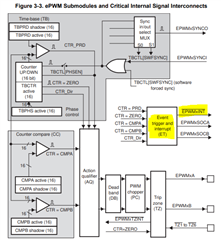
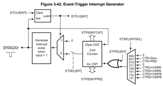
    For EPWM, there are many submodules, one of those being the Event Trigger submodule. This submodule is responsible for enabling the ePWM events that will trigger an interrupt. So in this case both lines of code are required for epwm interrupts. One is enabling the interrupt at the PIE level and the other at the IP level.

    // Enable EPWM1A INT in the PIE: Group 3 interrupt 1
    PieCtrlRegs.PIEIER3.bit.INTx1 = 1;
       	
    EPwm1Regs.ETSEL.bit.INTEN = 1;		// interrupt enable for ePWM1

    Best Regards,

    Marlyn

  • Hello Marlyn,

    My sincere apologies for replying after almost one entire month and I am actually thankful for your response.

    In your reply, you mention that we may use either of the following two lines:

    1) CpuTimer0Regs.TCR.all = 0x4000; // Use write-only instruction to set TSS bit = 0
    2) CpuTimer0Regs.TCR.bit.TSS = 0; // start timer0

    4000 (in line 1) makes the 14th bit (Timer Interrupt Enable) as 1, which in other words means that we have enabled/activated the TINT0 interrupt. But we are already doing that with the following declaration:

    EALLOW;
    PieVectTable.TINT0 = &cpu_timer0_isr;
    EDIS;
    PieCtrlRegs.PIEIER1.bit.INTx7 = 1;
    IER |=1;
    EINT;
    ERTM;

    I understood your explanation about ePWM interrupt activation and the methodology behind it as well but why enable/activate TINT0 twice? Because I was able to run the timer interrupt program just with the TSS = 0 option perfectly.

    Regarding me being unable to open up a new post I saw the following error message today:

    FORBIDDEN
    You don't have permission to access /idp/startSSO.ping on this server.

    What does this error message mean?

    I apologise yet again, however, I had one more query on the unexpected toggling behaviour of the GPxDAT register which was being handled by Matthew. Any idea why I am getting an unexpected output while toggling?

    With Regards,
    Ankit

  • Hi Ankit,

    No worries!

    The 'ConfigCpuTimer()' function which both sets of code call actually sets the TIE bit to 1 in order to enable the generation of a timer interrupt (this is through the timer's configuration). If this bit is not enabled then you are basically saying that you don't want the timer to be able to generate any interrupt signal. This is different from the following lines, in which we are enabling the CPU to service the interrupt (TINT0) that came from timer 0.

    EALLOW;
    PieVectTable.TINT0 = &cpu_timer0_isr;
    EDIS;
    PieCtrlRegs.PIEIER1.bit.INTx7 = 1;
    IER |=1;
    EINT;
    ERTM;

    why enable/activate TINT0 twice? Because I was able to run the timer interrupt program just with the TSS = 0 option perfectly.

    Since the TIE bit is already set within the ConfigCpuTimer() function then you can just start the timer through the TSS bit like you mentioned. However, if you change TSS through the TCR register and not the bit itself then you have to make sure not to clear the TIE bit (since this bit is part of the register and you are doing a register write) or else the timer will not generate any interrupts. 


    I will let follow up with the rest of your questions.

    Best Regards,

    Marlyn