This thread has been locked.

If you have a related question, please click the "Ask a related question" button in the top right corner. The newly created question will be automatically linked to this question.

TMS320F28069M: SCIB receiver error

Part Number: TMS320F28069M
Other Parts Discussed in Thread: SN65HVD485E,

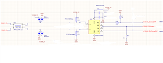
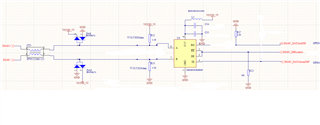
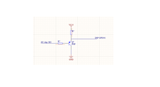
I use 28069M SCIB module to implement RS485 communication with a encoder based on modbus-rtu protocol. The 28069M board is customized. The 485chip is SN65HVD485.

GPIO40 is configured as SCITXDB;

GPIO41 is configured as SCIRXDB;

GPIO43 is configured as direction control;

MCU is as master, encoder is as slave.

SCIB transmitter interrupt and receiver interrupt are all enabled;

The transmitter buffer and receiver buffer level =2;

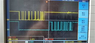
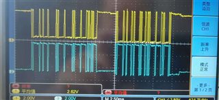
The current situation is that MCU transmitter seems ok because the encoder returned pulses out (If the transmitted pulses to encoder is not correct, then the encoder will not return out pulses).

But the receiver displays errors as below in CCS debug window:

Since the error generated, the receive interrupt can not be entered. 

How to solve that ? Any comment will be appreciated.

  • Hi,

    Thanks for your question! Given the BRKDT flag being set, I would suspect that the RX line is being pulled low for longer than expected (by the encoder).

    Can you verify by getting a scope plot of the SCI-RX/TX lines before and during the error condition?

    It would be a bit strange if the encoder's default TX output is low, but if that is the case (a scope plot will show this), then that would be the source of the error.

    Regards,

    Vince

  • Thanks for your answer. Today I get the scope as below:

    The channel 1 (yellow) is pulses on the TX of 28069 GPIO40; the channel 2 (blue) is pulses on the RX of 28069(GPIO41). 

    The current situation is transmit interrupt is working, but receive interrupt does not work since receive error occured.

    The Bode rate is 9600bps.  

    The below is SCIB module settings;

    void scib_fifo_init()
    {
    // The below is for SCI operation with rs485 encoder communication;
    ScibRegs.SCICCR.all =0x0007;     // 1 stop bit, No loopback
                                                           // No parity,8 char bits,
                                                           // async mode, idle-line protocol

    ScibRegs.SCICTL1.all =0x0003;      // enable TX, RX, internal SCICLK,
                                                              // Disable RX ERR, SLEEP, TXWAKE

    ScibRegs.SCICTL1.bit.RXERRINTENA =0;           // Receiver error interrupt enabled

    ScibRegs.SCICTL2.bit.TXINTENA =1;                  // Enable TXRDY interrupt;
    ScibRegs.SCICTL2.bit.RXBKINTENA =1;             // Enable RXRDY/BRKDT interrupt;
    ScibRegs.SCIHBAUD =0x0001;                            // 9600 baud @LSPCLK = 22.5MHz (90 MHz SYSCLK). Reset default: 90Mhz/4=22.5Mzh;
    ScibRegs.SCILBAUD =0x0024;                            // 24

    ScibRegs.SCICCR.bit.LOOPBKENA =0;              // Disable loop back
    ScibRegs.SCIFFTX.all=0xC022;                          // SCI reset; Transmit FIFO enable; Transmit FIFO interrupt level =2;
    ScibRegs.SCIFFRX.all=0x0022;                          // Receive FIFO interrupt level =2; interrupt disabled;
    ScibRegs.SCIFFCT.all=0x0;                                // FIFO transfer delay =0; (delay between one frame and the next frame)

    ScibRegs.SCIFFTX.bit.TXFFINTCLR =1;
    ScibRegs.SCIFFTX.bit.TXFIFOXRESET=1;       // Transmit FIFO reset;

    ScibRegs.SCIFFRX.bit.RXFIFORESET=1;        // Receive FIFO reset;
    ScibRegs.SCIFFRX.bit.RXFFINTCLR =1;
    ScibRegs.SCIFFRX.bit.RXFFIENA =1;             //

    ScibRegs.SCIPRI.bit.SOFT = 1;                        //Complete current receive/transmit
    //sequence before stopping
    ScibRegs.SCIPRI.bit.FREE = 0;
    ScibRegs.SCIFFRX.bit.RXFFIL =2;                   //Receive FIFO interrupt level =2;
    ScibRegs.SCICTL1.all =0x0023;                       // Transmit enable; Receive enable; Re-Enable SCI;
    }

    The below is receive interrupt subroutine:

    __interrupt void scibRxFifoIsr(void)

    {

          if((timer0_count ==0) && (signal_receive ==0)) 
         {
             if(count_receive <=3)
              {
                  Uint16 i;
                 for(i=0;i<2;i++)
                  {
                      receBuf[2*count_receive+i] = ScibRegs.SCIRXBUF.all; // Read data
                 }

               count_receive++;
             }

          else if(count_receive >=4) 
         {
               signal_receive =1;          
                 count_receive =0;          //reset
         }
       }

    ScibRegs.SCIFFRX.bit.RXFFOVRCLR=1;             // Clear Overflow flag
    ScibRegs.SCIFFRX.bit.RXFFINTCLR=1;               // Clear Interrupt flag
    PieCtrlRegs.PIEACK.all |=0x100;                          // Issue PIE ack

    }

    The below is timer interrupt subroutine, the communication period is 100ms. 

    __interrupt void timer0Isr(void)

    {
      if(timer0_count ==0)                              //90ms period reached, 10ms period start;
      {

             ConfigCpuTimer(&CpuTimer0, 90, 10000);               //config 10ms to start
             GpioDataRegs.GPBSET.bit.GPIO43 =1;                   //transmit direction enable
             timer0_count=1;                                                        //sign of sending time period
             signal_transmit =0;                                                   //enable sending
    }
    else if(timer0_count ==1)                      //10ms period reached, 90ms period start
    {
       ConfigCpuTimer(&CpuTimer0, 90, 90000);                //config 90ms to start
       GpioDataRegs.GPBCLEAR.bit.GPIO43 =1;               //receive direction enable
       timer0_count=0;                                                           //sign of receiving time period
       signal_receive=0;                                                         //enable receiving

    }

      CpuTimer0Regs.TCR.all = 0x4000;

    // Acknowledge this interrupt to receive more interrupts from group 1
    PieCtrlRegs.PIEACK.all |= PIEACK_GROUP1;

    }

    Please help me to identify the possible reasons, thank you.

  • Hi,

    Looks like the initial worry I had is correct: the encoder used in your project is pulling the F2806x RX line low during transmission. See red box around the problem in the image below.

    This is non-standard for UART protocol, and causes a break detect in the system. This is problematic because it will always cause errors like this.

    Unfortunately, this is therefore not an issue that is unique to F2806x, but any UART device RX that receives a break detect will flag it as either an error or as a special state.

    Because of this, please reach out to the encoder device's support team to determine the reason for this "low pulse", as that is the source and reason for the issue.

    Once the low pulse is removed from the encoder's output, all should work correctly!

    I would be happy to assist once the low pulse has been removed!

    Regards,

    Vince

  • Thanks, Vince:

    The waveforms pasted is at the pin of DSP Tx and Rx; These two pins are connected with DI and RO pin of  sn65hvd485. While sn65hvd485 A,B pins are connected with encoder output. the Hardware circuit that I used is as below:

    The scope pasted earlier is from RO pin and DI pin of 485 chip.

    And I have asked the encoder supplier the issues that you mentioned, they told me that the encoder output is standard RS485.  The scope I got is after the 485 chip, not the scope on the output of the encoder, so they guess the chip may have some problem. And today I have tested the encoder output,viz, the scope at the pin of A,B of sn65hvd485, the scope is as follows:

    The upper line is A pin of the 485 chip, the lower line is  B pin of the 485 chip.

    So it seems that the encoder output pulses are differentiated always, but after the 485 chip, the RO pin is low level during the DI pin is active transmitting (the scope pasted earlier).  So what happened? The circuit is wrong somewhere ? 

  • In addition, in the circuit, there are two resistors, R37, R38, this is used to divide the output voltage of 485 chip to be below 3.3V, since the chip is a 5V power supply chip, but 28069x is 3.3v and it is not 5v tolerant. I have take R38 out and disconnected with DSP pin , and test the pin RO directly, it is also low level during the DI is active transmitting. So it may conclude that the low level is not caused by R37 connected to gnd. 

  • So it may conclude that the low level is not caused by R37 connected to gnd. 

    The SN65HVD485E RO Receiver Output is High-impedance when its RE input is high; i.e. when the 28069x is transmitting on the RS485 half-duplex interface.

    The R37 which is part of the voltage divider on the Receiver Output will pull-down the signal when the 28069x is transmitting on the RS485 half-duplex interface.

    To avoid the receive errors, the GPIO41 receive pin on the 28069x needs to be pulled up when the 28069x is transmitting on the RS485 half-duplex interface.

    Given the need for the voltage divider to convert from the 5V SN65HVD485E output to the 3.3V 28069x not sure on the easiest way of achieving that.

  • Thanks Gillon,

    I will check the initialization of GPIO41 which is pulled-up enabled in 28069x internal settings; But I have even remembered that I have enable ot disable of the pin with pull-up settings, the same result have been got. Anyway, I will have a check and have a test once again. 

  • I will check the initialization of GPIO41 which is pulled-up enabled in 28069x internal settings;

    The TMS320F28069M datasheet shows that the typical current for a GPIO with the internal pull-up enabled is –140μA.

    With R37 being 2.2k, the typical pull-up current will result in 0.3V which is less than the VIL (max) of 0.8V and so will still be considered low.

    Perhaps replacing R37 with a 3.3V zener diode would both limit the input voltage to the 28069x and allow the internal pull-up to keep the receive signal high when the SN65HVD485E receiver is disabled.

  • Hi,

    Thank you for the circuit diagram, this greatly clears up the issue. As Chester rightly mentioned, the RX pin of the F2806x (which should be directly connected to RO of the transceiver) is being pulled down by the resistor divider shown.

    There are two best ways to solve this, unfortunately both of which require a re-work of the board unfortunately:

    1. Use a 5V capable transceiver (which should allow for the least effort and least cost increase). TI should have several RS-485 that would fit your needs here.

    -or-

    2. Use a communications voltage level-shifter to change from 5V logic (of F2806x) to 3V logic of the transceiver. This requires another chip and so is non-ideal.

    The reason I would recommend avoiding the resistor divider network entirely is because:

    1. The resistor divider is inherently pulling down the voltage given its tie to ground. This is the reason for the issue you are seeing.

    2. The inline resistance on RX pin (that is not on TX pin) causes a mismatch in resistance which is not ideal.

    And finally some clarity on your second set of waveforms: RS-485 is a differential communication, so the + and - will always be the opposite of one another. Data in and data out are always outputted on both lines.

    The transceiver simply takes the F2806x-RX and F2806x-TX UART data and converts UART protocol (single ended and 0 to 5V) to RS-485 protocol (differential +/- voltage). Unforuntately the transceiver that was chosen here is for 3V UART logic and needs to be changed to one that supports 5V logic for best out-of-the-box performance.

    Regards,

    Vince

  • Thanks for all your comments and explanations. Actually, I have mentioned that "the low level is not caused by R37 connected to gnd";  Today, I have a test on it to clarify that. 

    I have disconnected the R38 from the "RO" pin of sn65hvd495 chip and dsp "GPIO41" pin. then the circuit is like the below:

    Then I run the CCS program on it and test the waveforms on the pin of "RO" and "DI" of SN65HVD485, The results are as below:

    In the above plot, channel1 (yellow) is the waveform on "DI" pin of SN65HVD485 chip, which is the signal of DSP transmit out to the encoder; The channel2(blue) is the waveform of "RO" pin of SN65HVD485 chip, which is the signal of encoder transmit back to DSP.

    From the scope, we can see that there is still low level on the "RO" pin of Sn65HVD485 chip without connecting any resistors on that pin, which pin is now floating. 

    Therefore, it looks that the main reason of the "low level" is not caused by the resistors connected with the "RO" pin of sn65hvd485 chip.

    The below is the scope result of the "A,B" pin of sn65hvd485 chip for your reference, which is transmitted from encoder to sn65hvd485. 

  • Hi,

    The RO pin will still need a pull-up of its own (typically it uses the pull-up near the F2806x-RX pin, but now F2806x-RX has a pull-DOWN, and the transceiver RO pin is floating).

    RX pins (or the RO pin of the transceiver in this case) expect a pull-up of some kind. Please resolve this by one of the previously mentioned suggestions, and you will see the issue be resolved.

    Regards,

    Vince

  • Hi,

    Thanks, Vince and Gillion, the issue is resolved after I design a simple voltage level circuit on the output of 485 chip. The circuit like the below,

    I use a PNP transistor to realize 5v to 3.3v level shift.

    And I get the following waveforms on the DSP pins of SCIB;

    The SCI receiver interruptions work normally. Although the voltage level shift circuit is not perfect since it is almost maximum 4v pulses input to DSP pins seen from the scope.  I think this is caused by the voltage shift circuit which may not be well designed, but the issues has been resolved. 

    Once again, thanks all of you for your valuable  comments and suggestions to help me on that step by step.

    Thank you.