This thread has been locked.

If you have a related question, please click the "Ask a related question" button in the top right corner. The newly created question will be automatically linked to this question.

F28335 ADC Issue


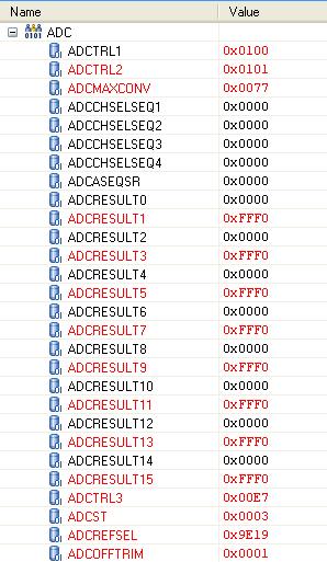
I have ADC conversion results issue. All odd indexed result registers (ADCRESULT1/3/5/.../13/15) reflect the results correctly, but the even indexed result registers (ADCRESULT0/2/6/.../12/14) are always zero. My configuration looks like  below.


//ADC reference register

AdcRegs.ADCREFSEL.bit.REF_SEL = AdcRefSel_Ext1_500V;


//ADCTRL3 configuration

AdcRegs.ADCTRL3.all = 0;

AdcRegs.ADCTRL3.bit.ADCBGRFDN = AdCtrl3BandgapRef_PU;

// Power up bandgap/reference/ADC circuits

DELAY_US(ADC_usDELAY);

AdcRegs.ADCTRL3.bit.ADCPWDN = AdCtrl3AdcCorePU;

// Power up ADC core

AdcRegs.ADCTRL3.bit.ADCCLKPS = AdCtrl3ClkPsDiv6;

// clk prescale

AdcRegs.ADCTRL3.bit.SMODE_SEL = AdCtrl3SampMode_Sim;

// sampling mode


//ADCTRL2 configuration

AdcRegs.ADCTRL2.all = 0;

AdcRegs.ADCTRL2.bit.EPWM_SOCA_SEQ1 = AdCtrl2PwmSoc_Enable;

// enable SOCA from ePWM to start SEQ1

AdcRegs.ADCTRL2.bit.EPWM_SOCB_SEQ2 = AdCtrl2PwmSoc_Enable;

// enable SOCB from ePWM to start SEQ2

AdcRegs.ADCTRL2.bit.INT_ENA_SEQ1 = AdCtrl2IntSeq_Disable;

// disable ADC Seq1 interrupt

AdcRegs.ADCTRL2.bit.INT_ENA_SEQ2 = AdCtrl2IntSeq_Disable;

// disable ADC Seq2 interrupt


//ADCTRL1 configuration

AdcRegs.ADCTRL1.all = 0;

AdcRegs.ADCTRL1.bit.SEQ_CASC = AdCtrl1SeqMode_DualSeq;

AdcRegs.ADCTRL1.bit.CPS = AdCtrl1Cps_Div1;

AdcRegs.ADCTRL1.bit.ACQ_PS = AQ_PS_2CLK;

AdcRegs.ADCTRL1.bit.CONT_RUN = AdCtrl1OpMode_StartStop;


// Setup continuous mode


//ADCMAXCONV configuration

AdcRegs.ADCMAXCONV.bit.MAX_CONV1 = 7;

// 8 channels on SEQ1

AdcRegs.ADCMAXCONV.bit.MAX_CONV2 = 7;

// 8 channels on SEQ2


DELAY_US(ADC_usDELAY);

//5ms delay before first convertion


AdcRegs.ADCCHSELSEQ1.all = 0x0000;

AdcRegs.ADCCHSELSEQ2.all = 0x0000;

AdcRegs.ADCCHSELSEQ3.all = 0x0000;

AdcRegs.ADCCHSELSEQ4.all = 0x0000;

Please refer to the ADC settings and results shown in the attachment.

Any ideas what was wrong?

  • Hi Louis,

    You have your ADC configured to sample in simultaneously. That means when there is SOC and you configured you wish to sample input A0, ADC will simultaneously sample A0 and B0, then convert A0 place it in result register, than it will convert B0 and place it in next result register. Therefore what you are seeing is values on A0 (0xFFF0) and B0 (0x0000) inputs

    Regards, Mitja

  • Mitja,

    Thank you for your response to my question, but it did not solve the problem. I had all channels tied to 3V power supply to test, as shown in the attachment, ADCRESULT0/2/4/.../12/14 got all 0, ADCRESULT1/3/5/.../13/15 got 0xFFF0. Then I configured all channels to channel 0, the results showed the same behaviour. Please offer other ideas.

  • Louis,

    The value of MAXCONV1 and 2 are incorrect for dual sequencer mode; it should be 0x0033 to get 4 double conversions, 8 total for each sequencer.  Please change to this and see if this corrects your results.  I'm not sure what the effect of 0x0077 will have in this mode.

    Additionally, can you send a schematic of your system?  As Mitja mentioned the results are showing 0V on ADCINA0 and 3V on ADCINB0 channels.

    Best,

    Matthew

  • Thank you all for your support. I attached a portion of my schematics pertinent to the ADC part. You may see that ADCINA0 and ADCINB0 and other channels are tied to 3V for testing purpose, and I also changed ADCMAXCONV to 0x0033, but I still get the same results: ADCRESULT0/2/4/.../12/14 are all zeros, ADCRESULT1/3/5/.../13/15 are 0xFFF0. There must be something wrong in the register configurations. Please help.