This thread has been locked.

If you have a related question, please click the "Ask a related question" button in the top right corner. The newly created question will be automatically linked to this question.

TMS320F2812: Error while debugging in H0 mode

Part Number: TMS320F2812

Hi,

I am trying to flash a custom F2812 board. The boot mode is H0. But during entering debugging, I receive the following error:

C28xx_CPU1: Failed CPU Reset: (Error - 1137@ 0x7). Device held in reset.

Please note the following:

1. I am able to get success in the JTAG integrity test.

2. When booted in H0, the XRS pin shows pulse wave. It shows 3.3 V only for 4.6ms and then is at 0V for 500ms, in a cyclic behaviour. 

3. When booted in Flash / SCI mode, XRS shows 3.3V all the time. 

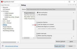
4. I have used latest CCS with XDS110.

5. I have used the ezdsp_ram_f2812 linker file.

  • Prasanna,

    Thanks for reaching out to the C2000 forum.  When you boot to H0, have you already loaded code to this region with the debugger?  If not, there will be uninitialized data in this area and the internal watchdog timer will eventually time out; issuing the reset pulse you see; which in turn will make it difficult for CCS to establish a connection.

    For the SCI boot mode, this will disable the WD as the device waits for data on the SCI port, so no WD reset will occur. 

    For the flash boot, if the device is new from TI this may behave very similar to the H0 boot, since from TI all flash is erased.  However, if you had programmed this region previously, then perhaps the watchdog is taken care of.

    The most reliable way to connect to this device is to enable the "Wait In Reset" mode inside your ccxml target config.  With this enabled the JTAG pod will drive EMU0/1 to a certain state that the C2000 will recognize when TRSTn pin goes inactive to hold the device until you can gain control.

    The SCI boot method would be my 2nd option if you have issues with the WIR mode.

    Best,

    Matthew

  • Hi Matthew,

    Thanks for the inputs. I understood the mistake. Essentially we need to halt the processor when connected to JTAG.

    I have some followup question regarding WIR Mode:

    1. Currently I have EMU0 and EMU1 pulled to 3.3V using a 3.3 k Ohm. 

    2. I am not able to see the "Power-On-Reset Mode" & "JTAG nTRST Boot-Mode" setting on target configuration for XDS110. This setting seems to be available on xds100Vx. Can I do this using modification in the ccxml file directly? If yes some reference would be helpful

    3. I also tried to set "Halt target on connect" in the debug setting of my project. It didnt help.

    4. Currently I have configured the EMU pins using a PU for EMU1 (3.3k) & PD(3.3k) for EMU0 as required to halt the processor. This is done on the debugger cable pcb. Seems to be working fine. Let me know if this is recommended or there if there is a better way.

    5. In case none of the above is working will i have to take the processor in SCI boot mode for loading the code to H0 and then switch the processor back to H0 bootmode for execution?

  • Prasanna,

    #4 option is fine(external pulls to activate WIR), this is what the emulator is supposed to do, but if this is not an option on XDS110 then an external drive is the only option.

    EMU0/1 are only latched by the device on rising edge of TRSTn; so leaving the pulls on the PCB is not an issue that will cause any impact to the device when it is free running(TRSTn = low).

    After you have loaded your code, you should be able to disconnect the debugger and pulse XRSn and the H0 boot should work correctly.

    Best,

    Matthew