Part Number: C2000WARE
Other Parts Discussed in Thread: POWERSUITE
Hi,
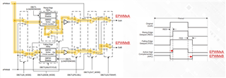
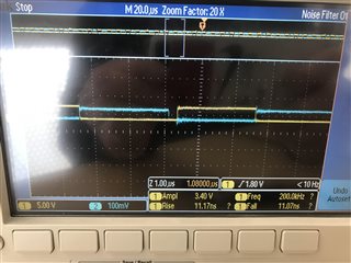
I am still having an issue in my C2000Ware code for the F2837xD device. When programming the dead-band modules of the PWM for EPWM 1 and EPWM 3, both outputs have overlapping PWM signals. I have attached such example photo of EPWM1 which uses HRPWM and has 1MHz output switching frequency:
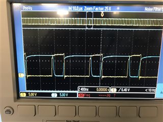
As you can see there is clear overlap here. I was thinking it could be that my gate driver rise and fall times are not the best, however it looks like even the command to turn on/turn off are overlapping, so it is most likely still a code problem as well. Here is my PWM set up for channel A/B of PWM1 module:
// PWM Generator Definitions
uint16_t FLY_PERIOD = 199; // Calculation: FCLK/FSW >> (200MHz/1MHz) - 1 = 199.
uint16_t FLY_DEADTIME = 8; // Dead-time generation = 8 x 5ns = 40nS
void InitEPwm1(void)
{
// Setup time-base
EPwm1Regs.TBCTL.bit.CTRMODE = 0; // Up count mode
EPwm1Regs.TBPRD = FLY_PERIOD; // Set timer period
EPwm1Regs.TBCTL.bit.PHSEN = 0; // Disable phase loading
EPwm1Regs.TBPHS.bit.TBPHS = 0; // Phase is 0
EPwm1Regs.TBCTR = 0; // Clear counter
// Set TBCLK = EPWMCLK = 100MHz
// Although the system clock is 200MHz
// maximum EPWM clock is 100MHz
EPwm1Regs.TBCTL.bit.HSPCLKDIV = 0; // Clock ratio to SYSCLKOUT
EPwm1Regs.TBCTL.bit.CLKDIV = 0;
EPwm1Regs.TBCTL.bit.SYNCOSEL = 0x0; // Do not synchronise output
// Initial modulation in Counter Compare Module
EPwm1Regs.CMPA.bit.CMPA = 10; // Set compare A value initially to zero (we will want to soft-start)
EPwm1Regs.CMPA.bit.CMPAHR = (1 << 8); // Initialise HRPWM extension
EPwm1Regs.CMPB.bit.CMPB = 100;
EPwm1Regs.CMPB.bit.CMPBHR = (1 << 8);
// Set actions in the action qualifier module
EPwm1Regs.AQCTLA.bit.CAU = 0x1; // Force PWMA low on count up
EPwm1Regs.AQCTLA.bit.ZRO = 0x2; // When TBCTR = ZRO, force PWMA high
EPwm1Regs.AQCTLB.bit.CBU = 0x2;
EPwm1Regs.AQCTLB.bit.ZRO = 0x1;
EPwm1Regs.DBCTL.bit.OUT_MODE = 3; // Fully enable dead-band for both falling and rising-edges
EPwm1Regs.DBCTL.bit.POLSEL = 2; // Active High Complimentary (AHC) Mode
//EPwm1Regs.DBFEDHR.bit.DBFEDHR = FLY_DEADTIME; // Set dead-time for falling edge
//EPwm1Regs.DBREDHR.bit.DBREDHR = FLY_DEADTIME; // Set dead-time for rising edge /* BEEN CHANGED BY JM HOLLAND */ TO HR BITS
EPwm1Regs.DBFED.bit.DBFED = FLY_DEADTIME;
EPwm1Regs.DBRED.bit.DBRED = FLY_DEADTIME;
EALLOW;
// Digital Compare (DC) Submodule
// Generate DCAH signal from Trip Combination Input
EPwm1Regs.DCTRIPSEL.bit.DCAHCOMPSEL = 15; // OR together all Trip combinations selected by DCALTRIPSEL Registers -> DCAH
EPwm1Regs.DCTRIPSEL.bit.DCBHCOMPSEL = 15; // OR together all Trip combinations selected by DCALTRIPSEL Registers -> DCBH
// DCAH/DCAEVT1/2 are used for one-shot trip faults
// DCBH/DCBEVT1/2 are used for cycle-by-cycle faults
// Individually select which trip signals are passed into the block to be ORed together
EPwm1Regs.DCAHTRIPSEL.bit.TRIPINPUT5 = 1; // Input Over Voltage Trip One-Shot Fault
EPwm1Regs.DCAHTRIPSEL.bit.TRIPINPUT7 = 1; // Cathode Over Voltage Trip One-Shot Fault
EPwm1Regs.DCBHTRIPSEL.bit.TRIPINPUT4 = 1; // Fly-back Over Current Trip Cycle-by-Cycle Fault
// Event A Action Qualifier block
// Generate DCAEVT1/DCBEVT1 trip events according to DCAH and DCBH
// Only EVT1 can be used for OST, and EVT2 for CBC
// Need to enable both A and B of these registers to trigger both the PWMx outputs
EPwm1Regs.TZDCSEL.bit.DCAEVT1 = 2; // DCAEVT1: DCAH = high, DCAL = don't care
EPwm1Regs.TZDCSEL.bit.DCAEVT2 = 2; // DCAEVT2: DCAH = high, DCAL = don't care
EPwm1Regs.TZDCSEL.bit.DCBEVT1 = 2; // DCBEVT1: DCBH = high, DCBL = don't care
EPwm1Regs.TZDCSEL.bit.DCBEVT2 = 2; // DCBEVT2: DCBH = high, DCBL = don't care
// Event Triggering block - Generate DCAEVT1.force and DCBEVT1.force signals (One Shot Source)
EPwm1Regs.DCACTL.bit.EVT1SRCSEL = 0; // Select DCAEVT1 as input signal
EPwm1Regs.DCACTL.bit.EVT1FRCSYNCSEL = 1; // Select Asynchronous
EPwm1Regs.TZFRC.bit.DCAEVT1 = 0; // Enable DCAEVT1.force output signal
EPwm1Regs.DCBCTL.bit.EVT1SRCSEL = 0; // Select DCBEVT1 as input signal
EPwm1Regs.DCBCTL.bit.EVT1FRCSYNCSEL = 1; // Select Asynchronous
EPwm1Regs.TZFRC.bit.DCBEVT1 = 0; // Enable DCBEVT1.force output signal
// Event Triggering block - Generated DCAEVT2.force and DCBEVT2.force signals (Cycle-by-Cycle Source)
EPwm1Regs.DCACTL.bit.EVT2SRCSEL = 0; // Select DCAEVT2 as input signal
EPwm1Regs.DCACTL.bit.EVT2FRCSYNCSEL = 1; // Select Asynchronous
EPwm1Regs.TZFRC.bit.DCAEVT2 = 0; // Enable DCAEVT2.force output signal
EPwm1Regs.DCBCTL.bit.EVT2SRCSEL = 0; // Select DCBEVT2 as input signal
EPwm1Regs.DCBCTL.bit.EVT2FRCSYNCSEL = 1; // Select Asynchronous
EPwm1Regs.TZFRC.bit.DCBEVT2 = 0; // Enable DCBEVT2.force output signal
// Trip Zone Submodule - Trip Logic block
// Using only TZCTL and EVT1
EPwm1Regs.TZCTL2.bit.ETZE = 0; // Use only TZCTL register, disable TSCTL2
EPwm1Regs.TZCTL.bit.DCAEVT1 = 0x10; // On trip, force EPWM1A to a LOW state
EPwm1Regs.TZCTL.bit.DCBEVT1 = 0x10; // On trip, force EPWM1B to a LOW state
EPwm1Regs.TZCTL.bit.DCAEVT2 = 0x10; // On trip, force EPWM1A to a LOW state
EPwm1Regs.TZCTL.bit.DCBEVT2 = 0x10; // On trip, force EPWM1B to a LOW state
EPwm1Regs.TZCTL.bit.TZA = 0x10; // On trip, force EPWM1A to a LOW state
EPwm1Regs.TZCTL.bit.TZB = 0x10; // On trip, force EPWM1B to a LOW state
// Trip-Zone Submodule - select OSHT and CBC sources
EPwm1Regs.TZSEL.bit.DCAEVT1 = 1; // Enable DCAEVT1 as one-shot-trip source for this ePWM module
EPwm1Regs.TZSEL.bit.DCBEVT1 = 1; // Enable DCBEVT1 as one-shot trip source for this ePWM module
EPwm1Regs.TZSEL.bit.DCAEVT2 = 1; // Enable DCAEVT2 as a CBC trip source for this ePWM module
EPwm1Regs.TZSEL.bit.DCBEVT2 = 1; // Enable DCBEVT2 as a CBC trip source for this ePWM module
//EPwm1Regs.TZFRC.bit.OST = 0x01; // Force trip to disable PWM outputs
//EPwm1Regs.TZFRC.bit.CBC = 0x01; // Force cycle-by-cycle trip to disable PWM outputs
// May insert code which either waits a delay time before clearing the one-shot fault, or something along those lines
// At the moment, I believe, this will turn OFF the PWM module until user-reset.
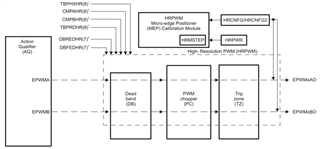
// High Resolution Pulse Width Modulator Definitions
EPwm1Regs.HRCNFG.all = 0x0; // Clear all bits first within the HRCNFG register
EPwm1Regs.HRCNFG.bit.EDGMODE = 0x3; // Control both falling and rising edge delays with the MEP
EPwm1Regs.HRCNFG.bit.CTLMODE = 0x0; // CMPAHR controls the MEP
EPwm1Regs.HRCNFG.bit.HRLOAD = 0x0; // Shadow load on CTR = Zero for count-up mode
EPwm1Regs.HRCNFG.bit.AUTOCONV = 1; // Enable auto-conversion logic
EPwm1Regs.HRPCTL.bit.HRPE = 0; // Turn off high-resolution period control
EDIS;
// Set up ADC trigger pulse to ADC SOCA (ADCAINT1)
EPwm1Regs.ETSEL.bit.SOCAEN = 0; // Disable SOCA on A group
EPwm1Regs.ETSEL.bit.SOCASEL = 2; // Select SOCA on period match
EPwm1Regs.ETSEL.bit.SOCAEN = 1; // Enable SOCA
EPwm1Regs.ETPS.bit.SOCAPRD = 1; // Generate pulse on 1st event
}
Is there anything blatantly wrong with this code above? The PRD is 199, and dead-time is 8 so about 40nS for a 1uS period. I have tried smaller dead-times to no avail, facing the same issues.
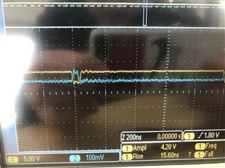
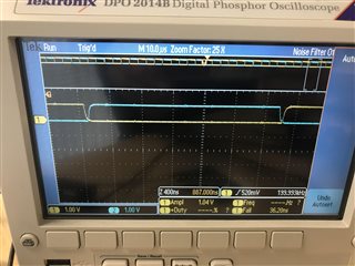
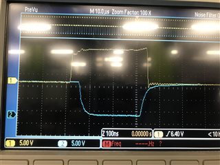
Any advice is appreciated, and any other information I can provide I will do so happily. Here's a closer look at the signals;
Best regards,
Joel