This thread has been locked.

If you have a related question, please click the "Ask a related question" button in the top right corner. The newly created question will be automatically linked to this question.

TMS320F280049: TIDA-00961 product page

Part Number: TMS320F280049
Other Parts Discussed in Thread: SFRA

Hello C2000 Gurus,

Is TIDA-00961 (1.6kW GaN based TotemPole PFC design) not supported anymore? I could not find any information on it on ti.com. Is the documentation and software archived someplace users have access to?

Thanks,

Hrishi

  • Hrishi,

    Someone from TI will contact you regarding access to this material, we've taken it offline for the time being as you have noticed.

    Best,

    Matthew

  • Thanks Matt! I appreciate your quick response. 

    I was looking for this because I came across a post by  from earlier this year: https://e2e.ti.com/support/microcontrollers/c2000-microcontrollers-group/c2000/f/c2000-microcontrollers-forum/1008597/tms320f280049-zvs-question-about-tida-00961/3731337#3731337

    I have answered his questions in a new post here: https://e2e.ti.com/support/microcontrollers/c2000-microcontrollers-group/c2000/f/c2000-microcontrollers-forum/1061022/tms320f280049-answer-to-zvs-question-on-tida-00961

    Please let me know if you come across any other unanswered questions on this design. I will be happy to help.

    Best,

    Hrishi

  • Hi Hrishi I have some questions

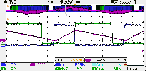
    Question 1: Regarding the control logic, I noticed that 00961 does not use the ZCD circuit to detect the moment when the inductor current changes from negative to zero to drive the main switch. It seems that a predictive control is used to configure the ton and toff of the next cycle. As well as the period and dead zone, directly use the epwm module to generate the duty cycle. I don't know why this method is used, or is there any advantage in this method, compared with ZCD. In addition, in this way, will the main switch be turned on when the resonance is not completed?

  • Supplement the picture of question one  It seems that the main switch is turned on before the resonance is over. At this time, the inductor current also seems to oscillate.(This phenomenon occurred after I increased the input frequency )

  • Question 2: Regarding the small signal modeling of the totem pole Crm working mode, how did you solve it at that time?

  • Question 3: Why do we need different ton_adjusted calculation formulas for the rising phase and the falling phase of the inductor current? In addition, for the calculation of toff, it seems that ton_calc is used to calculate the volt-second balance instead of ton_adjusted. Why is that?

  • Sorry for asking so many questions at once, because the delisting of this project has caused me a lot of confusion. There is no place to ask for advice. I am very happy to see your post. Thank you!

  • Hi Wei,

    I can understand your frustration because this is a very complex design. Hopefully TI will be able to make this design go live again soon.

    As I explained in my other post https://e2e.ti.com/support/microcontrollers/c2000-microcontrollers-group/c2000/f/c2000-microcontrollers-forum/1061022/tms320f280049-answer-to-zvs-question-on-tida-00961 the Toff value is adjusted every cycle to approach ZVS based on the detection of presence or absence of ZVS. You can think of the calculated Toff value as being the 'coarse' adjustment, while the ZVS detection based adjustment to be the 'fine' adjustment to achieve/approach ZVS. The whole point of this approach is to avoid using direct ZCD detection, which can be unreliable around the noise prone zero crossing.

    You mentioned that you saw oscillations on the inductor current at higher input frequency. What was the input frequency? Please do not increase it beyond the design specifications.

    Not sure about question 2. I believe I used the SFRA and compensation designer tools to help close the loops.

    I believe the ton_adjusted is related to the duty preservation function when ZVS adjustment is applied (see my other post mentioned above). This is to provide seamless transitions in and out of the toff adjustment mode without distorting the input current waveform. 

    I hope this helps.

    Best,

    Hrishi

  • thank you! 

    This control method without ZCD seems to rely on accurate calculation of ton toff and dead zone. For 50hz input, 50khz interrupt seems to be sufficient, but for higher input frequency (for example, I increased the input to 400) , I found that there may be inaccurate dead zones and  toff calculations, which will cause problems when the main switch (ton) is turned on, just like the waveform of my question 1.

  • Please do not connect a 400Hz input to this system! This design only accepts input AC signal with a frequency between 47Hz and 63Hz (Universal AC input). Please see the input specs below:

    Best,

    Hrishi

  • Hi Hrishi

    Regarding my question 3, I don't quite understand why the asym_fact factor should be added to the rising edge of the inductor current. In addition, at uin<0.5Uo, ton_adj_dbg is introduced to compensate for the negative current at the zero crossing. I can understand it. But why not use the overall ton insist of ton_adj_dbg to calculate  toff  here, but use the ton calculated by the loop to calculate the toff.

  • This is to provide seamless transitions in and out of the toff adjustment mode without distorting the input current waveform

    Can you elaborate on the meaning of this passage

  • Hi Wei,

    Regarding ton_adj_dbgThis is related to the transitions around the input (50/60Hz) voltage/current zero crossing. From what I remember the boost action is stopped around the zero crossing and then a weightage factor is used once it kicks back in after the start of the next input half cycle. This helps improve pf and thd numbers.

    Best,

    Hrishi

  • seamless transitions in and out of the toff adjustment mode without distorting the input current waveform

    The mode I am talking about is when ZVS adjustment is used (Toff adjusted). This mode could be entered and exited during a half cycle of the input voltage/current waveform. When the ZVS adjustment is not used in part of the half cycle, the duty cycle of the active switch results in a certain input current wave shape. Once the ZVS toff adjustment is added, the duty cycle is disturbed and can cause input current waveform distortion in the half cycle at the mode transition point. The amount of distortion depends on the amount of adjustment. With the duty preservation algorithm, this distortion is minimized considerably.

    I hope this helps.

    Best,

    Hrishi

  • Thank you, I noticed the PCB schematic of 00961  You named these signals ZCDxxx. Does this mean that your original plan was to detect the ZCD signal to give a turn-off signal. Because as far as I know, theoretically speaking, when uin>0.5uo, the extra conduction time of toff can be deduced. Why not directly add to the calculation formula of toff, but adopt this kind of ZVS loop scheme

  • We considered some approaches at the beginning and stuck to the one that worked the best. Yes, toff can be deduced but you cannot solely rely on calculations, specially at high switching frequencies where even a small deviation from the calculation (because of parasitics, tolerances, and such) can have a big impact on the result. We go all the way up to 1.2MHz of switching on this design.

    Best,

    Hrishi  

  • Hi Hrishi.

    I noticed that there is a crossover signal in the schematic, but it doesn't seem to be used in practice. I would like to ask, what was this signal originally used for?

  • Regarding the issue of the ZVS loop, I noticed that the ZVS loop is only allowed to run when the output is greater than 370V. Then I adjusted this value to 170V. I wanted to take a look at the low input, but I found that it didn't work. I don't know the reason. I hope to get your guidance.

    In addition, although theoretically speaking, in the area of uin<0.5Uo, the circuit can naturally achieve ZVS, but I have noticed some situations. When the rectifier is turned off, the inductor current has not yet dropped to 0, and there is even It takes a long time to drop to 0, which will waste the dead time and affect the resonance time, which may cause ZVS not to be achieved in the uin<0.5Uo area.

  • By the way, with regard to the processing of zero-crossing points, why do we need to detect currents instead of using phase-locked loops for all processing, and are there any particulars about the selection of the range of zero-crossing points (phase-locked loop greater than 0.03)

  • Hi Wei,

    Like some of the other circuits on this design, the crossover circuit was for experimentation and not used in the final release. A software PLL is used to detect zero-crossing points and that is why external circuit is not required for this purpose.

    This design has been optimized to work for output voltage range specified in the specifications sections and intended for specific target applications. This design will need to be changed considerably (firmware and hardware) for it to work outside these specifications. It is not recommended to operate this design outside its specifications.

    Best,

    Hrishi

  • Thank you Hrishi

    I have some questions about the hardware part of the ZVS detection loop.

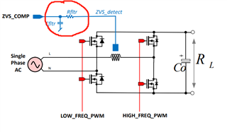
    This schematic diagram is the part of the circuit that realizes the ZVS detection. After the voltage across the auxiliary winding passes through the capacitor and the rectifier bridge, it should be able to reflect the soft switching of the switch tube vds.

    1,But what is the L302 that follows, and I want to ask what it does?

    This picture comes from a ppt introducing 00961. The red circle is the CR differential circuit that detects the slope change. I performed simulation based on the principle shown in the figure, and the simulation found that the circuit as shown in the figure cannot detect the sudden change in slope, but if the position of the capacitor and the resistance are exchanged, the sudden change in slope can be successfully detected. I don’t know what the reason is.

     Attach a partial picture of my simulation in simulink

    One last question: What are C and R in the CR differential circuit in the top schematic? Are they C204? But when the blank signal is 1, isn't C204 short-circuited? I hope you can talk about the hardware principles of this part in detail.

  • Hi Wei,

    We are not detecting the slope. Please refer to my earlier explanation of how the presence or absence of ZVS is detected.

    Blank signal is not used, instead on-chip blanking logic on the F28004x is used. C204 is not populated because the ADC anti-aliasing cap on the control card is used for this filtering.

    Hope this answers all your questions.

    Best,

    Hrishi

  • Hi Hrishi

    I know that only ZVS1_2 is used in the design. It uses a CR circuit to detect the voltage across the auxiliary winding of the inductor. If ZVS is not achieved, there will be spikes.

     my question is: what is the function of L302?(In my understanding, L302 should be a capacitor, which forms the CR circuit for detection together with R206

  • Hi Hrishi

    I used Gpio to test the operation of the interruption of pwmisr, and found that the waveform has some problems. The green is the interrupted waveform, and the blue is the high-frequency drive waveform. According to my understanding of this part of the code, three high-frequency drives should trigger an interrupt. But judging from the actual test waveform, it is inconsistent with my understanding. If my understanding is wrong, I look forward to your guidance. Thanks!

  • The PWM ISR does not run continuously. It only runs if/when the control ISR commands a change in frequency or duty. Once the PWM ISR is triggered, it may retrigger 2 times or 3 times, depending on the amount of change in duty/freq and to make sure the change is seamless at the PWM output. This retrigger of the PWM ISR occurs at the rate of fsw/3.

    Hope this helps.

    Hrishi

  • Thank you Hrishi, it really helped me!

    And I have some other questions。

    This waveform diagram is about the debugging of the ZVS detection part. The dark blue line is the operation status of the PWMISR output by me using gpio. Light blue is the inductor current. The three-channel red line is the zvs_lost signal I output with the DAC. The four-channel green line is the output that I put the Cmpss output to the Gpio port using outX-bar.

    Obviously, it can be seen that when PWMISR is running (dark blue line is high), there is no ZVS signal (the green line has pulses), but the zvs_lost signal (red) is 0 at this time. This means that the pulse has not been detected. I have been confused about this problem for a long time, and I don't know the reason. I want to know your views and suggestions, thank you!

  • I feel that I have not said in detail enough on this question, because I want to test the accuracy of ZVS detection, so I deleted the code that added toff in the uin>0.5uo area in the code.

    If you have any doubts about my approach, please let me know.Help your answer!