This thread has been locked.

If you have a related question, please click the "Ask a related question" button in the top right corner. The newly created question will be automatically linked to this question.

TMS320F28069M: Custom Board Design failing Lab 01c

Part Number: TMS320F28069M
Other Parts Discussed in Thread: DRV8301, MOTORWARE, DRV8316

Hello,

I'm checking out our own board design, based heavily on the DRV8301-HC-EVM Rev D. I'm going through the Insta-Spin labs.

I've already run through most of the labs with the evaluation kit. I can run Lab 01b with no problems - speed even tracks pretty closely with set-point.

My problems start when I close the current loop. The motor is very shaky and haltingly turns a fraction of a revolution at a time.

It also gets pretty hot after a few minutes. (This may or may not be related, but I don't see much activity on the SPI bus between

the micro and the DRV8301. The chip select line goes low for 3ms, but I can't see any data being transferred.) Lab 01c is ostensibly

for verifying signal chain integrity. But no clues are given in the lab regarding what to do if the motor doesn't spin properly. What specifically

is meant in this instance by "signal chain integrity" and if the integrity of the signal chain is compromised or damaged, or some error is present,

how should I troubleshoot it such that I can isolate the "link" in the chain that is responsible?

Thanks,

Dave

  •  Please try to follow the steps to verify the hardware, you may check if step 2 and step 3 are right since you can run the lab01b.

    1. Change the PWM and ADC configuration in hal.c refer to the guide, motorware_hal_tutorial.pdf.

    C:\ti\motorware\motorware_1_01_00_18\docs\tutorials


    2. Set correct parameters based on the hardware board in user.h

    #define USER_IQ_FULL_SCALE_VOLTAGE_V           (xx)

    #define USER_VOLTAGE_FILTER_POLE_Hz               (xx)

    #define USER_ADC_FULL_SCALE_VOLTAGE_V       (xx)

    #define USER_IQ_FULL_SCALE_CURRENT_A           (xx)

    #define USER_ADC_FULL_SCALE_CURRENT_A       (xx)


    3. make sure that the sign of the current coefficient in HAL_readAdcData() in hal.h matches the current sensing circuit. Refer to chapter 5.2.2 Current Feedback Polarity in InstaSPIN user's guide (SPRUHJ1, https://www.ti.com/lit/spruhj1) to set the sign of the current scale factor.


    static inline void HAL_readAdcData(HAL_Handle handle,HAL_AdcData_t *pAdcData)

    {

       _iq current_sf = (+/-)HAL_getCurrentScaleFactor(handle);

    }


    4. Follow the instaSPIN lab guide to use lab01b and lab01c to verify your own hardware since you are not using the TI EVM kits and then run the subsequent labs.


    5. Using the lab02b or lab02c to identify the motor parameters, and use the identified parameters to run the motor if the current and voltage sensing signals are verified and good.

  • Thanks Yanming. I'll try everything you've listed.

    Best Regards,

    Dave

  • OK. Close this thread first. Let's know if have any further question.

  • Hi Yanming,

    I've been spinning these motors for some time, using the DRV8301-HC-EVM evaluation kit. I'm pretty sure I have all the parameters in user.h at good values (may need to tweak some of them a little). The sign of the scale factor is correct (negative feedback, so offsets are positive). I can run the motor in Lab01b. The graphs generated don't bear much resemblance to those in the Lab guide. They're very "choppy" looking, as though the sampling rate just isn't fast enough. But that's true whether I perform the lab with my custom board or with the evaluation board.

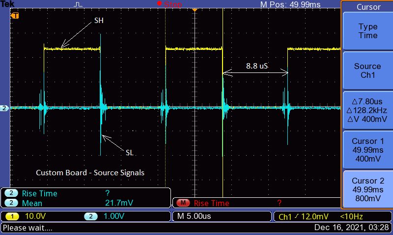
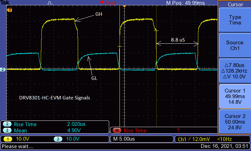
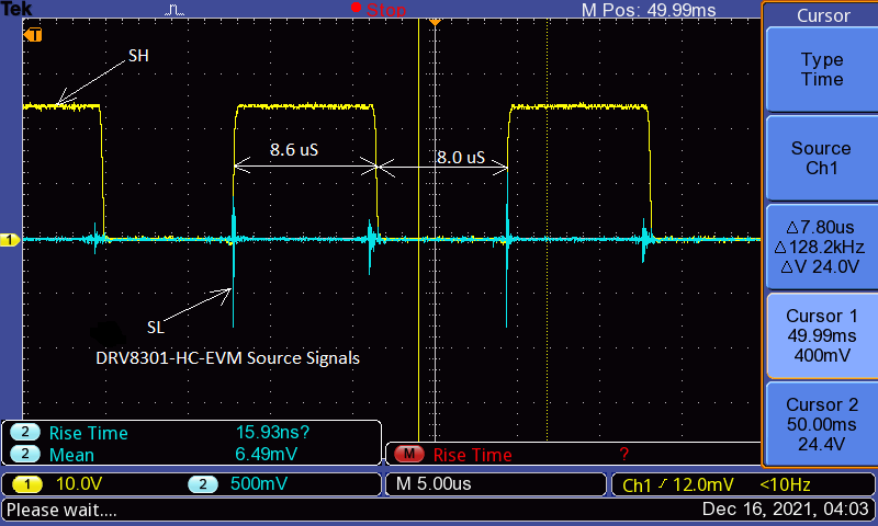
    I've noticed that the waveforms associated with the FETs are somewhat different on my board, as compared to the evaluation board. I've attached some screen shots from the scope. It looks like the EVM has a much softer turn on at the gates. Maybe the gate capacitance on the FETs I've chosen is too low? I haven't compared the actual values from the data sheets, but I'll do that next. Also, the transient ringing on the current sense line is much larger and wilder on my board than on the EVM, but that may be a consequence of the FETs snapping On and Off so rapidly.

    Thanks for your help.

    Best Regards,

    Dave

  • You may have a look at the datasheet of DRV8301, and find some application notes on TI website. You can follow the recommendation to design the driver board for motor control.

  • Hi Yanming,

    Thanks for the reply. However, I was hoping for some help regarding the information provided above.  Do you think that FETs that turn On / Off too quickly could cause the problems I described in the first item of this exchange? Does the ringing on the source pin of the low FET (high end of current sense resistor) look excessive to you? Is there anything I can do to mitigate this problem without entirely redesigning the board? That is, could I put a capacitor on the gate, or something like that - something that would get me through testing This board? Then I could make any required changes (perhaps selecting different FETs)  permanent on the next spin. Would adjusting dead-time help with these issues? What Application Notes do you suggest?

    Thanks,

    Dave

  • You may take a look at the following application notes. If you still have any questions about the hardware design, please create a new thread, the expert of the DRV device will give the answer to you.

    System Design Considerations for High-Power Motor Driver Applications

    Understanding Smart Gate Drive (Rev. D)

  • Thanks Yanming!

    Is there some way I could transfer this whole conversation over to a DRV8301 forum?

    Best Regards,

    Dave

  • Yes, re-assigned to DRV team for support this topic.

  • Thank you. So should I look in the Motor Drivers forum for this topic?

    Best Regards,

    Dave

  • Hi Dave,

    I am the DRV83x expert from the BLDC motor drivers team. Thanks for reaching out. 

    In regards to your gate drive waveforms on your custom board vs eval board, it looks like you have much less input capacitance for your MOSFET gates or higher gate drive current from the DRV8301. I have not worked with the DRV8301-HC-KIT before or know what the default gate drive setting is from the control card, but please try using a lower gate drive setting or add series gate resistors if you can to see if that improves performance. 

    Slamming the FETs on/off too fast causes ringing and poor EMI performance, and can affect current switching and torque control if you switch the currents too fast. 

    Thanks,
    Aaron

  • Hi Aaron,

    Thanks for the advice. I agree that the gate capacitance is much lower for the FETs I'm using, compared to the DRV8301-HC kit. They seem to be way too snappy in almost every way. Also, the Rds(on is considerably higher:

                         BSO150N03MDG (my FET)             SUM110N06-3m9H (used on EVM)
    Rds(on)                    0.015 ohm                                              0.0039 ohm
    Ciss                            970 pF                                                  15,800 pF

    I will definitely try out your suggestions. By "gate drive setting," I assume you mean the peak gate drive current, which is adjustable on the DRV8301?

    I've been reading your presentation How_to_do_BLDC_Schematic_Review_and_Debug.pptx, along with the commented mock schematic, etc... You've put together a very helpful package there - thank you. I noticed that you mentioned a couple of times

    "Do NOT connect SNA, SNB, SNC directly to GND; this will sense GND noise rather than the voltage at the low-side of the shunt resistor." The EVM kit appears to make a direct connection to ground, but they may have taken other measures to mitigate noise.

    In my case I'm connecting SP1, SP2 and SP3 directly to ground, since I'm using negative feedback. So, how should I avoid a direct ground connection? Should I put another resistor in series with the sense resistor? The sense resistor is 2 milli ohms. Would a duplicate resistor be the way to go?

    Thanks,

    Dave

  • Hi Dave,

    Glad you discovered those resources, I was about to suggest those next! And yes, by gate drive setting, I am referring to peak gate drive current. You can calculate the approximate VDS rise/fall times by this equation: Qgd / I_gate = t_rise. If capacitance is lower, your Qgd value of your FETs should be lower too. Rise/fall times <100ns are generally considered really fast and should be avoid when switching large currents to avoid electrical overstress and EMI. 

    Few things in mind I've discovered with DRV8301 in regards to overcurrent:
    - OC_ADJ_TH overcurrent settings have +/-20% error
    - OC_ADJ_TH settings < 0.125V could have more than 20% error depending on process variation
    - Overcurrent is monitored from PVDD1-SHx for the HS, which is not very accurate compared to newer gen devices because PVDD1 is not a dedicated drain sense pin

    That is okay to use negative feedback, but SPx/SNx should connect to the pads of the shunt resistor and routed differentially to the DRV8301 (Kelvin connection) for accurate shunt feedback so GND noise is not picked up into the CSAs. Using a net-tie is helpful in these situations. 


    Please also check out these resources on system design considerations for higher power motors: https://e2e.ti.com/support/motor-drivers-group/motor-drivers/f/motor-drivers-forum/1012824/faq-system-design-considerations-for-high-power-motor-driver-applications

    Thanks,
    Aaron

  • Hi Aaron,

    Ok - I see what you mean. I'm already using Kelvin connections to just "sip" off the main current carrier. But the diff-amp is not nearly as close to the source as shown in your drawing. I'm having trouble locating just how to change the peak current for the 8301 in the EVM code, so I'll probably start with increasing the gate resistance - I'm using 1 ohm right now. Thanks for the link and thanks for your help! Have a great weekend.

    Dave

  • Hi Dave,

    Sure thing! Please mark as resolved if this solved your issue. Have a good weekend!

    THanks,
    Aaron

  • Hi Aaron,

    I did finally figure out how to change the peak gate current. There are evidently 3 values available 1.7A, 0.7A & 0.25A. It was set to 1.7A by default in the InstaSpin code. Tried both of the other two, to little, if any, effect. I also doubled the gate resistance from 1 ohm to 2. I think maybe the noise at the current sense amps was damped down a little, but my original problems still remain (see first entry in this discussion). Should I increaINFNS16227-1.pdfse the gate resistance even further? I've attached the data sheet for the FETs I'm using; perhaps you can suggest a gate resistance, or provide me with a procedure for determining what resistance I should use?

    Thanks,

    Dave

  • Hi Dave,


    Thanks for sharing MOSFET datasheet. These still have a low Qgd (1.4nC), so gate drive current of 250mA still yields a fast turnon/turnoff time of 5.9ns assuming no gate resistance. The datasheet says Rg = 1 ohm, however this will not add much gate current limitation. Unfortunately there is not an easy way at the moment to calculate gate resistance vs gate current, so trial and error remains the best solution. 

    I would bump up the resistors to 50-100 ohms, see if this improves the waveforms to what the DRV8301-HC-EVM Rev D does. 

    Thanks,
    Aaron

  • Thanks Aaron - just knowing a general range is a big help!

    Dave

  • Sure thing Dave, let me know if any more help is needed. 

    Thanks,
    Aaron

  • Hi Aaron,

    I've tried various values of Rbase. Here are the qualitative results:

    100 ohm -  Supply current went up considerably and the system shut down after a few seconds.

                       Didn't capture any waveforms; I was too hung up on getting something to work.

                       Besides, they were gone in an instant.

                       From what I could see, though, the gate drive voltage climb was much more moderate, especially toward the peak,

                       which makes the behavior all the more puzzling. Maybe a large spike develops across the base resistor, since the R

                       is so large. Anyway, I didn't dare take it any higher.

    47 ohm -  Pretty much the same as 100 ohm.

    18 ohm  - Acts about the same as when a 2 ohm resistor in place - very snappy turn-on and turn-off.

                     Didn't think to capture any waveforms here either.

    27 ohm - Climb of waveform at gate appears gentler than with 1 ohm or 2 ohm. Much more rounded at the top - rise time about

                    a quarter of a microsecond.

                   The resistor seems to have made less of an impact on turn-off, however. Looks like a bit less ringing on the current sense signal.

                   The motor, however, is behaving as badly as ever - very shaky and haltingly turns a fraction of a revolution at a time.

                   It also gets pretty hot after a few minutes. This is while running lab 01c of the InstaSpin Labs.

    Thanks,

    Dave

  • Hi Dave,

    The GLx rise time looks good (~400ns). The ringing at the sense resistor does not look good, there is a lot of ringing that does not settle until after 1us. Which gain setting is used, and does it match with the table below?


    If the motor is behaving worse, my guess is that current feedback is not good. I think that this was also the original issue on the DRV8301-HC-EVM kit. To confirm there's not an issue at the powerstage, monitoring GH_x, SH_x, GL_x, and SL_x for each phase is good to ensure the gate drive waveforms switch correctly and not switch too fast. 

    Is deadtime being implemented? If so, can dead time be removed and does this help?

    If the waveforms appear good with no known issues, I would plot SNx vs SPx to see if there is large ringing at the resistor when current is switching. Ringing can be caused to parasitic inductance in the layout of the board, grounding, or placement/size/package of the sense resistor(s). A filtering cap between SNx and SPx (~1nF) may help too with dampening ringing. Also applying an RC filter at the output of the CSA (SOx) can help filter noise from the signals from motor switching. 

    I think investigating schematic and layout may also help, can you share with me? Feel free to send over PM as well if you would not like to share publicly. 

    I will be out of office until 1/3/2022, so please be patient with any replies on this thread. 

    Thanks,
    Aaron

  • Hi Aaron,

    Do you mean the gain of the CSA amps? They're set up with a gain of 20, so the rise time should be 600ns, as opposed to 450 or so.

    Dead-time is being used in a very minimal way. There's a 1 ohm resistor from DTC to ground. Would it make much difference if I shorted that out?

    The ringing shows up everywhere to some degree, including power and ground...

    I have dummy locations for RC filtering at the CSA outputs. I'll give that a try.

    I think you're right; it's probably a layout issue. At the very least, I'm probably going to have to bring the DRV8031 closer to the sensing/FET bridge, and route the SNx and SPx lines more carefully.

    I'll send you the schematic & layout via PM.

    Thanks for your help & Merry Christmas and a Happy New Year!

    Best Regards,

    Dave

  • Hi Dave,

    Thanks for posting your question to e2e - please give us some time to investigate this further

    Responses may be delayed a bit due to the team being out during holiday timeframe 


    Best Regards, 
    Andrew

  • Hi Andrew,

    Aaron already explained that he'll be out 'til Jan 3rd. Starting tomorrow, I'm out until the 4th, so no problem.

    Thanks,

    Dave

  • Hi Dave, 

    understood and hope you have a nice holiday break!

    (f.y.i for e2e metrics, we have to have the latest response in the thread, so that the thread is marked as attended/resolved) 

    Best Regards, 
    Andrew 

  • Hi Dave,

    I'm back from vacation now. Yes, I was referring to the CSA amp gain = 20, looks the scope capture shows the CSA settling around 600ns. 

    Changing the DTC resistor from 1 ohm to GND shouldn't change much and dead time should stay around 50ns. 

    Can you please share schematic and/or layout over PM if possible to glance over?
    Minimizing parasitic inductance from the DRV8301 to the power stage is the best way to have a robust power stage. If long, thin gate drive output traces exist, then it can have adverse effects when sourcing and sinking higher magnitudes of gate drive current. 

    These app note should help with PCB layout for higher power designs:
    System Design Considerations for High-Power Motor Driver Applications
    Best Practices for Board Layout of Motor Drivers

    Regards,
    Aaron

  • Hi Aaron,

    Happy New Year! Hope you had a good vacation. 

    Just got back from xmas break today. I sent you the schematics, etc..., using the "Send a private message" selection when hovering over your photo, above.

    If you didn't get it let me know, and I'll resend. I don't have the layout in front of me right now, but I'm pretty sure the gate drive runs are long and skinny.

    Thanks for the advice and the App notes.

    Beat Regards,

    Dave

  • Hi Dave,

    Can you resend? I do not have anything in my inbox at the moment. 

    Thanks,
    Aaron

  • Tried it again, and noticed that when I click on "Send a private message", it sends me to a page that doesn't refer to Aaron Barrera, instead "admin" is shown at the top.

    Dave

  • Hi Aaron,

    So is there some other step I'm missing? Should I email subscribe? Or request friendship?

    Dave

  • Hi Dave, 

    I received it, I will investigate review it and give you a reply tomorrow. 

    Thanks,
    Aaron

  • Hi Dave,

    I provided you feedback over PM on your layout. There are lots of comments I made because with the current layout, there are lots of possibilities from a layout perspective that can negatively impact your motor driver performance with InstaSPIN-FOC. Top concerns are:

    - Placement of charge pump and voltage regulator capacitors around DRV8301
    - Gate drive traces are very thin, long, and go through multiple vias (adds inductance to switching current paths)
    - 1/2-bridge MOSFET package prohibits larger copper areas for motor current to dissipate, adds inductance to motor switching and can results in noise in phase voltage/current required for InstaSPIN-FOC

    Thanks,
    Aaron

  • Thanks for all the advice! The first two I can definitely fix. For the third, could I use the same FETs, just widen the traces once I get a little ways out from the pin?

  • Hi Dave, 

    You could use the same FETs, I would just recommend using polygon pours in the PCB software to widen the high current traces as much as possible. Also try to route high current copper pours through multiple layers as well, this reduces inductance and improves thermal dissipation for the DRV8301 and FETs as well. 

    Please review these application notes:
    System Design Considerations for High-Power Motor Driver Applications
    Best Practices for Board Layout of Motor Drivers

    One other thing to note, since your application uses 24V,  8-A peak current, a new device you could evaluate is the DRV8316, which is an integrated 3-phase MOSFET BLDC driver that supports up to 40-V abs max, 8-A peak current. It includes 3x integrated CSAs, 3.3V/5V buck regulator, LDO, and SPI or hardware interface. 

    Thanks,
    Aaron

  • Thanks Aaron,

    Working on  new layout now. Would you mind giving it another look once I'm done? I'll mark this resolved, and contact you through PM once it's 'complete.'

    Thanks,

    Dave