Part Number: TMS320F28388D
Other Parts Discussed in Thread: BOOSTXL-POSMGR, TIDM-1010, CONTROLSUITE
Hi all,
I know the SDK is not released for BISS-C Encoder using F28388D but I am planning on having multiple BISS-C encoders wired to the F2838D in the future.
I am working on a design with several GPIO accessible on a connector and I would like to make sure the non configurable/fixed pins needed for BISS-C communication are available on the connector.
First of all based on the BOOSTXL-POSMGR/TIDM-1010 with the F28379D launchpad I assume that the max number of biss-c encoders wired to the F28xxxx is 4 (using 2xBOOSTXL) :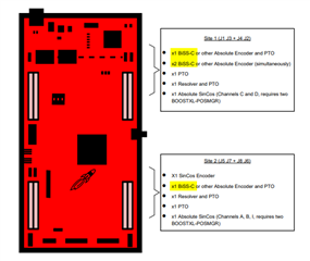
Can you confirm we cannot have more than 4 biss-c wired to a F283xxx? What is the reason/limitation?
What does "x2 BiSS-C or other Absolute Encoder (simultaneously)" means?
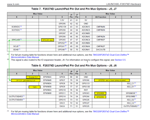
Now for the pins/ressources needed, everything is confusing and I am not sure what is configurable and what is not.
Based on the schematic of the BOOSTER and pins associated on the launchpad I got the pins listed in the table: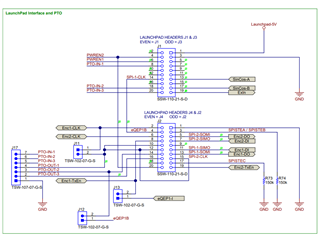
| Enc1-CLK | GPIO0 | |
| CLB-SPICLK | GPIO1 CAN YOU CONFIRM | |
| SPI1-CLK | GPIO60 | SPIA |
| SPI1-SIMO / Enc1-DI | GPIO58 | SPIA |
| SPI1-SOMI / Enc1-DO | GPIO59 | SPIA |
| Enc1-TxEn | GPIO3 | |
| Enc2-CLK | GPIO2 | |
| CLB-SPICLK | GPIO5 CAN YOU CONFIRM | |
| SPI2-CLK | GPIO124 | SPIC |
| SPI2-SIMO / Enc2-DI | GPIO122 | SPIC |
| SPI2-SOMI / Enc2-DO | GPIO123 | SPIC |
| Enc2-TxEn | GPIO29 | |
| Enc3-CLK | GPIO6 | |
| CLB-SPICLK | GPIO7 | |
| SPI3-CLK | GPIO65 | SPIB |
| SPI3-SIMO / Enc3-DI | GPIO63 | SPIB |
| SPI3-SOMI / Enc1-DO | GPIO64 | SPIB |
| Enc3-TxEn | GPIO9 | |
| Enc4-CLK | ? | |
| CLB-SPICLK | ||
| SPI4-CLK | ? | |
| SPI4-SIMO / Enc4-DI | ? | |
| SPI4-SOMI / Enc4-DO | ? | |
| Enc4-TxEn | ? |
Could you tell me which pins is fixed vs which is configurable? I looked at the code example C:\ti\controlSUITE\development_kits\BOOSTXL_POSMGR\v01_01_00_00\bissc-F28379DLpad-S2\examples\PM_bissc_SystemTest in biss.c and I see GPIO24,25,26,27 are commented and they use GPIO63,64 and 65, so I guess I can change all SPI pins as long as SPIB stays SPIB right?
For the last encoder 4, I don't know which pin to use, SPID for SOMI SIMO CLK but what will be the dedicated Enc4-CLK Enc4-TxEn and CLB-SPICLK?
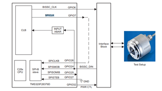
Why the schematic does not reflect the image below? I don't see the Enc-TxEn that enable the transceiver, is it a mandatory signal or it is only use if it is a bi-directional communication?
Thank you