Other Parts Discussed in Thread: TMS320F28335
Dear Sir,
I am designing new hardware for AD2S1205 resolver reading device with C2000 processor.
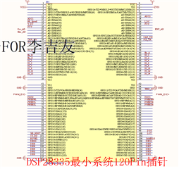
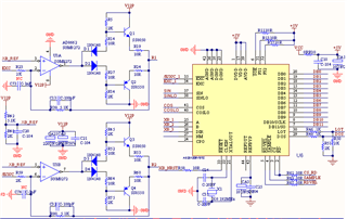
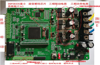
I have a reference schematics from Chinese EVAL-KIT for FOC motor drive with Resolver Decoding.
The AD2S1205 data of resolver position can be read from Signal DB-0 to DB-11 in 12-bits resolution.
(EXTERNAL MEMORY INTERFACE, The data is MSB first.)
However, the evaluation board schematics are connected not in sequencing like my though.
They are connected like below.
-----------------------------------------
TMS320F28335 :: AD2S1205
-----------------------------------------
XD2 :: DB11
XD1 :: DB10
-----------------
XD4 :: DB09
XD3 :: DB08
-----------------
XD6 :: DB07
XD5 :: DB06
-----------------
XD8 :: DB05
XD7 :: DB04
-----------------
XD10 :: DB03
XD9 :: DB02
-----------------
XD12 :: DB01
XD11 :: DB00
-----------------
AS you may see above, they are connected revesingly, and vice versa in pair.
(For reversing connection, it is making sense for data MSB first.)
But Why it need to connect vice versa in pair, Does anyone have any idea for this reason?
Thank you in advance
Happy Chrismas !!
Narudol T.