This thread has been locked.

If you have a related question, please click the "Ask a related question" button in the top right corner. The newly created question will be automatically linked to this question.

TMS320F280049-Q1: Opamp powered by 5V to buffer GPIO

Part Number: TMS320F280049-Q1
Other Parts Discussed in Thread: TINA-TI

Hi team,

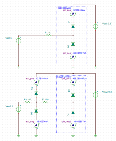
Is there any concern if opamp buffer to GPIO is powered by 5V (which is exceeding 3.6V rating) to buffer a 2.5V DC voltage to C2000? In the case of opamp failure, or 2.5V failure, there is a possibility of having >3.6V at GPIO pin. 

How about to use an external series resistor (say >2.5kohm) to limit any potential current injected to the pin <2mA? Is this acceptable? 

  • Hi PY,

    Are you driving a GPIO or an analog input pin?  

    I think if you are driving a GPIO, then using a level shifter would be better/safer?  This should take care of preventing an over-voltage on the lower voltage side. 

    If you are driving an analog input, then yes, you can limit the current with a series resistor.  However, note that series resistance on the analog input will slow down S+H settling, which is very undesirable for driving an ADC input, see https://www.ti.com/lit/an/spract6/spract6.pdf

    Some other options for an analog/ADC input:

    You can add some external clamping diodes such that the circuit is op-amp --> R1 --> external diodes --> R2 --> Analog input pin / internal clamping diodes.  You can then set R1 and R2 to steer most of the current to the external diodes in case of the fault you are describing.  This should reduce the overall resistance of R1 + R2 vs. the previous case you described. 

    Use an op-amp with an enable,  and disable the op-amp if one or either power rail is bad.   You can do something similar, but gate the whole 5V power rail with a regulator with enable or with a power FET.   

  • Hi Devin,

    Thank you! Do you have simplified diagram for below? I don't quite understand how the circuit looks like. Thank you! 

    • You can add some external clamping diodes such that the circuit is op-amp --> R1 --> external diodes --> R2 --> Analog input pin / internal clamping diodes.  You can then set R1 and R2 to steer most of the current to the external diodes in case of the fault you are describing.  This should reduce the overall resistance of R1 + R2 vs. the previous case you described. 
  • Hi PY,

    I've pasted some a quick TINA-TI simulation below.

    In the first case, we only use a 1k external resistor to limit the current to the internal diodes.  This does a good job (a little over 1mA flows into the device with 5V applied) but the overall series resistance is 1kohm, which is moderately high for driving an ADC input.

    In the second case, an external set of diodes has been added (note: if you are only worried about over-voltage situation, you can omit the low-side diode to VSSA).  R3 is added to limit the current as before, but it can be smaller because the external diodes are generally rated for much higher current.  R2 is then added to steer current to the external diodes instead of the internal diodes.  Overall, the series resistance is now only 200 ohms (and the current going into the device has been reduced as well).

    Note that this is just a quick simulation to show that this circuit will reduce the overall series resistance.  You'd want to spend a little more time engineering the circuit to ensure that (1) The clamping current to the external diodes and internal device diodes are always within specification (2) the amount of clamping current won't cause issues for your op-amp and (3) the components on the ADC input can allow for a S+H time that is acceptable for the application.   

    Also note that the control cards use some external diode packs that might be a starting place if you are looking for a way to effectively protect many ADC inputs.  

    Ext_Diodes.TSC

  • Hi Devin,

    This is clear! Thank you!