This thread has been locked.

If you have a related question, please click the "Ask a related question" button in the top right corner. The newly created question will be automatically linked to this question.

TMS320F28388D: Missing a PWM cycle on all channels

Part Number: TMS320F28388D

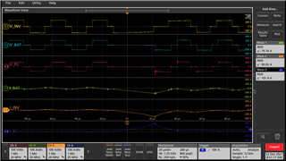
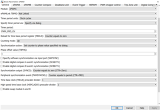
I am using EPWM1 to EPWM6 with switching frequency of 30 kHz and EPWM7 with switching frequency of 120 kHz. PWMs are synched with the master (ePWM1). Deadband is 1 us. CMPA and CMPB are constant and equal to half of the cycle. When some of the phase shifts get close to zero, we randomly miss a whole cycle on all the PWMs other than the main one. ePWM2, ePWM4 and ePWM 6 have phase shifts that are higher than half cycle and ePMW3 and ePWM4 have small phase shifts when the random skipping of cycles happens.

  • It's most likely caused by setting the PHASE SHIFT and skipping an action which then seems like you have skipped a cycle.

  • Thanks for the reply Nima. If that is the case why all PWM channels with low and high phase shift numbers are missing the action? It only makes sense to either have ePWM2, ePWM4 and ePWM 6 miss a cycle or have ePMW3 and ePWM4 miss a cycle.

  • Most likely because you write to them sequentially. The order is probably what's causing some to fail due to the time it occurs.

  • so ePWM1 which is the first one does not receive any phase shifts. It always has phase shift of zero but that also does not turn on in that cycle. The upper switch turns off and gives the negative pulse voltage but then the upper switch is supposed to turn on after half a cycle and it does not. Do you think the counter can have an Anatoly for one switching cycle?

  • I dont think there is an anamoly in your counter. I think its a miss configuration in your code. So for EPWM1 you have PHSEN=0 and you are seeing this issue?

  • I used code generation of Simulink and I have set the phase shift of ePWM1 to 1 instead of zero. Here is the code:

    EPwm1Regs.TBPHS.all = (EPwm1Regs.TBPHS.all & ~0xFFFF0000) | 0x10000;
  • Then you still have the PHSEN set to "enabled" mode. That could be what is causing this. Do you have the generated code?

    If you are using MATLAB, I recommend you ask this on their forum.

    Nima

  • I deactivated the phase shift for ePWM1 (the main one) and it ran well with a set of our high voltage DC supplies. When I changed the supplies it started having issues again. Do you think the noise on 3.3 supply or the ground can cause an issue like this?

    I have actually measured 3.3 V to ground and here is what I got:

  • I dont think the noise is the issue based on your capture. Is this a custom board?

    Nima

  • Yes it is a custom board. 

    Here is our code for ePWM1:

      /* S-Function (c2802xpwm): '<S1>/ePWM' */


            /*-- Update CMPA value for ePWM1 --*/

            {

              EPwm1Regs.CMPA.bit.CMPA = (uint16_T)(rtb_Switch2);

            }

    /*rtb_Switch2 and rtb_Switch3 comes from a analog switch that is connected to a GPIO pin and a software set variable.

            /*-- Update CMPB value for ePWM1 --*/

            {

              EPwm1Regs.CMPB.bit.CMPB = (uint16_T)(rtb_Switch3);

            }

    EPwm1Regs.TBCTL.all = (EPwm1Regs.TBCTL.all & ~0x3FCF) | 0x0;

          EPwm1Regs.TBCTL2.all = (EPwm1Regs.TBCTL2.all & ~0xC000) | 0x0;

          /* // Time-Base EPWMxSYNCOUT Source Enable Register

             EPwm1Regs.EPWMSYNCOUTEN.bit.ZEROEN      = 1; // Sync Output Select

           */

          EPwm1Regs.EPWMSYNCOUTEN.bit.SWEN = 0;// disable the SWEN enabled during reset

          EPwm1Regs.EPWMSYNCOUTEN.all = (EPwm1Regs.EPWMSYNCOUTEN.all & ~0x2) | 0x2;

          /*-- Setup Time-Base (TB) Submodule --*/

          EPwm1Regs.TBPRD = 6664;          // Time Base Period Register

    EPwm1Regs.TBPHS.all = (EPwm1Regs.TBPHS.all & ~0xFFFF0000) | 0x0;

          // Time Base Counter Register

          EPwm1Regs.TBCTR = 0x0000;        /* Clear counter*/


        EPwm1Regs.CMPCTL.all = (EPwm1Regs.CMPCTL.all & ~0x3C5F) | 0x0;

    EPwm1Regs.CMPCTL2.all = (EPwm1Regs.CMPCTL2.all & ~0x3C5F) | 0x0;

          EPwm1Regs.CMPA.bit.CMPA = 3332;  // Counter Compare A Register

          EPwm1Regs.CMPB.bit.CMPB = 3332;  // Counter Compare B Register

          EPwm1Regs.CMPC = 0;              // Counter Compare C Register

          EPwm1Regs.CMPD = 0;              // Counter Compare D Register


          EPwm1Regs.AQCTLA.all = 146;

    EPwm1Regs.AQCTLB.all = 2564;

          EPwm1Regs.AQSFRC.all = (EPwm1Regs.AQSFRC.all & ~0xC0) | 0x0;

          EPwm1Regs.AQCSFRC.all = (EPwm1Regs.AQCSFRC.all & ~0xF) | 0x0;

      EPwm1Regs.DBCTL.all = (EPwm1Regs.DBCTL.all & ~0x8FFF) | 0xB;

          EPwm1Regs.DBRED.bit.DBRED = (uint16_T)(200.0);

                             // Dead-Band Generator Rising Edge Delay Count Register

          EPwm1Regs.DBFED.bit.DBFED = (uint16_T)(200.0);

    EPwm1Regs.ETSEL.all = (EPwm1Regs.ETSEL.all & ~0xFF7F) | 0x9901;

          EPwm1Regs.ETPS.all = (EPwm1Regs.ETPS.all & ~0x30) | 0x30;

          EPwm1Regs.ETSOCPS.all = (EPwm1Regs.ETSOCPS.all & ~0xF0F) | 0x101;

          EPwm1Regs.ETINTPS.all = (EPwm1Regs.ETINTPS.all & ~0xF) | 0x1;

          EPwm1Regs.PCCTL.all = (EPwm1Regs.PCCTL.all & ~0x7FF) | 0x0;

    EALLOW;

          EPwm1Regs.TZSEL.all = 0;         // Trip Zone Select Register


          EPwm1Regs.TZCTL.all = (EPwm1Regs.TZCTL.all & ~0xFFF) | 0xFFF;

          EPwm1Regs.TZEINT.all = (EPwm1Regs.TZEINT.all & ~0x7E) | 0x0;


          EPwm1Regs.DCACTL.all = (EPwm1Regs.DCACTL.all & ~0x30F) | 0x4;

          EPwm1Regs.DCBCTL.all = (EPwm1Regs.DCBCTL.all & ~0x30F) | 0x0;

          EPwm1Regs.DCTRIPSEL.all = (EPwm1Regs.DCTRIPSEL.all & ~ 0xFFFF) | 0x0;

          EPwm1Regs.TZDCSEL.all = (EPwm1Regs.TZDCSEL.all & ~0xFFF) | 0x0;


    EPwm1Regs.DCFCTL.all = (EPwm1Regs.DCFCTL.all & ~0x3F) | 0x10;

          EPwm1Regs.DCFOFFSET = 0;         // Digital Compare Filter Offset Register

          EPwm1Regs.DCFWINDOW = 0;         // Digital Compare Filter Window Register

          EPwm1Regs.DCCAPCTL.all = (EPwm1Regs.DCCAPCTL.all & ~0x1) | 0x0;

          EPwm1Regs.HRCNFG.all = (EPwm1Regs.HRCNFG.all & ~0xA0) | 0x0;


          EPwm1Regs.EPWMXLINK.bit.TBPRDLINK = 0;

          EPwm1Regs.EPWMXLINK.bit.CMPALINK = 0;

          EPwm1Regs.EPWMXLINK.bit.CMPBLINK = 0;

          EPwm1Regs.EPWMXLINK.bit.CMPCLINK = 0;

          EPwm1Regs.EPWMXLINK.bit.CMPDLINK = 0;


          EPwm1Regs.HRPCTL.all = (EPwm1Regs.HRPCTL.all & ~0x72) | 0x2;

          EDIS;


     Code for ePWM2:

    /* S-Function (c2802xpwm): '<S1>/ePWM2' */

            EPwm3Regs.TBPHS.bit.TBPHS = rtb_RoundingFunction6;

            /*-- Update CMPA value for ePWM3 --*/

            {

              EPwm3Regs.CMPA.bit.CMPA = (uint16_T)(rtb_Switch2);

            }

            /*-- Update CMPB value for ePWM3 --*/

            {

              EPwm3Regs.CMPB.bit.CMPB = (uint16_T)(rtb_Switch3);

            }

    EPwm3Regs.TBCTL.all = (EPwm3Regs.TBCTL.all & ~0x3FCF) | 0x4;

          EPwm3Regs.TBCTL2.all = (EPwm3Regs.TBCTL2.all & ~0xC000) | 0x0;

          EPwm3Regs.EPWMSYNCOUTEN.all = (EPwm3Regs.EPWMSYNCOUTEN.all & ~0x1) | 0x1;

          EPwm3Regs.TBPRD = 6664;          // Time Base Period Register

          EPwm3Regs.TBPHS.all = (EPwm3Regs.TBPHS.all & ~0xFFFF0000) | 0x0;

          EPwm3Regs.TBCTR = 0x0000;        /* Clear counter*/

          EPwm3Regs.CMPCTL.all = (EPwm3Regs.CMPCTL.all & ~0x3C5F) | 0x0;

      EPwm3Regs.CMPCTL2.all = (EPwm3Regs.CMPCTL2.all & ~0x3C5F) | 0x0;

          EPwm3Regs.CMPA.bit.CMPA = 3332;  // Counter Compare A Register

          EPwm3Regs.CMPB.bit.CMPB = 3332;  // Counter Compare B Register

          EPwm3Regs.CMPC = 0;              // Counter Compare C Register

          EPwm3Regs.CMPD = 0;              // Counter Compare D Register

          EPwm3Regs.AQCTLA.all = 146;

          EPwm3Regs.AQCTLB.all = 2564;

          EPwm3Regs.AQSFRC.all = (EPwm3Regs.AQSFRC.all & ~0xC0) | 0x0;

          EPwm3Regs.AQCSFRC.all = (EPwm3Regs.AQCSFRC.all & ~0xF) | 0x0;

      EPwm3Regs.DBCTL.all = (EPwm3Regs.DBCTL.all & ~0x8FFF) | 0xB;

          EPwm3Regs.DBRED.bit.DBRED = (uint16_T)(200.0);

          EPwm3Regs.DBFED.bit.DBFED = (uint16_T)(200.0);
    EPwm3Regs.ETSEL.all = (EPwm3Regs.ETSEL.all & ~0xFF7F) | 0x9901;

          EPwm3Regs.ETPS.all = (EPwm3Regs.ETPS.all & ~0x30) | 0x30;

          EPwm3Regs.ETSOCPS.all = (EPwm3Regs.ETSOCPS.all & ~0xF0F) | 0x101;

          EPwm3Regs.ETINTPS.all = (EPwm3Regs.ETINTPS.all & ~0xF) | 0x1;

          EPwm3Regs.PCCTL.all = (EPwm3Regs.PCCTL.all & ~0x7FF) | 0x0;

    EALLOW;

          EPwm3Regs.TZSEL.all = 0;         // Trip Zone Select Register


    EPwm3Regs.TZCTL.all = (EPwm3Regs.TZCTL.all & ~0xFFF) | 0xFFF;

          EPwm3Regs.TZEINT.all = (EPwm3Regs.TZEINT.all & ~0x7E) | 0x0;

          EPwm3Regs.DCACTL.all = (EPwm3Regs.DCACTL.all & ~0x30F) | 0x4;

          EPwm3Regs.DCBCTL.all = (EPwm3Regs.DCBCTL.all & ~0x30F) | 0x0;

          EPwm3Regs.DCTRIPSEL.all = (EPwm3Regs.DCTRIPSEL.all & ~ 0xFFFF) | 0x0;

          EPwm3Regs.TZDCSEL.all = (EPwm3Regs.TZDCSEL.all & ~0xFFF) | 0x0;

         EPwm3Regs.DCFCTL.all = (EPwm3Regs.DCFCTL.all & ~0x3F) | 0x10;

          EPwm3Regs.DCFOFFSET = 0;         // Digital Compare Filter Offset Register

          EPwm3Regs.DCFWINDOW = 0;         // Digital Compare Filter Window Register

          EPwm3Regs.DCCAPCTL.all = (EPwm3Regs.DCCAPCTL.all & ~0x1) | 0x0;

          EPwm3Regs.HRCNFG.all = (EPwm3Regs.HRCNFG.all & ~0xA0) | 0x0;

      EPwm3Regs.EPWMXLINK.bit.TBPRDLINK = 2;

          EPwm3Regs.EPWMXLINK.bit.CMPALINK = 2;

          EPwm3Regs.EPWMXLINK.bit.CMPBLINK = 2;

          EPwm3Regs.EPWMXLINK.bit.CMPCLINK = 2;

          EPwm3Regs.EPWMXLINK.bit.CMPDLINK = 2;

    EPwm3Regs.HRPCTL.all = (EPwm3Regs.HRPCTL.all & ~0x72) | 0x2;

          EDIS;


  • Disable the phase shift on epwm1 and see if it works. Send me the updated code with TBPSH disabled so I can verify you disabled it.

  • It is already disabled by 

    EPwm1Regs.TBPHS.all = (EPwm1Regs.TBPHS.all & ~0xFFFF0000) | 0x0;

            /*-- Update CMPA value for ePWM1 --*/
            {
              EPwm1Regs.CMPA.bit.CMPA = (uint16_T)(rtb_Switch2);
            }
    
            /*-- Update CMPB value for ePWM1 --*/
            {
              EPwm1Regs.CMPB.bit.CMPB = (uint16_T)(rtb_Switch3);
            }
                 EPwm1Regs.EPWMSYNCOUTEN.bit.SWEN = 0;// disable the SWEN enabled during reset
          EPwm1Regs.EPWMSYNCOUTEN.all = (EPwm1Regs.EPWMSYNCOUTEN.all & ~0x2) | 0x2;
          
             /*-- Setup Time-Base (TB) Submodule --*/
          EPwm1Regs.TBPRD = 6664;          // Time Base Period Register
              /* // Time-Base Phase Register
             EPwm1Regs.TBPHS.bit.TBPHS               = 0;          // Phase offset register
           */
          EPwm1Regs.TBPHS.all = (EPwm1Regs.TBPHS.all & ~0xFFFF0000) | 0x0;
    
          // Time Base Counter Register
          EPwm1Regs.TBCTR = 0x0000;        /* Clear counter*/
          
             EPwm1Regs.CMPCTL.all = (EPwm1Regs.CMPCTL.all & ~0x3C5F) | 0x0;
    
          /* EPwm1Regs.CMPCTL2.bit.SHDWCMODE           = 0;          // Compare C Register Block Operating Mode
             EPwm1Regs.CMPCTL2.bit.SHDWDMODE           = 0;          // Compare D Register Block Operating Mode
             EPwm1Regs.CMPCTL2.bit.LOADCSYNC           = 0U;          // Active Compare C Load SYNC Option
             EPwm1Regs.CMPCTL2.bit.LOADDSYNC           = 0U;          // Active Compare D Load SYNC Option
             EPwm1Regs.CMPCTL2.bit.LOADCMODE           = 0U;          // Active Compare C Load
             EPwm1Regs.CMPCTL2.bit.LOADDMODE           = 0U;          // Active Compare D Load
           */
          EPwm1Regs.CMPCTL2.all = (EPwm1Regs.CMPCTL2.all & ~0x3C5F) | 0x0;
          EPwm1Regs.CMPA.bit.CMPA = 3332;  // Counter Compare A Register
          EPwm1Regs.CMPB.bit.CMPB = 3332;  // Counter Compare B Register
          EPwm1Regs.CMPC = 0;              // Counter Compare C Register
          EPwm1Regs.CMPD = 0;              // Counter Compare D Register
    
          /*-- Setup Action-Qualifier (AQ) Submodule --*/
          EPwm1Regs.AQCTLA.all = 146;
                                   // Action Qualifier Control Register For Output A
          EPwm1Regs.AQCTLB.all = 2564;
                                   // Action Qualifier Control Register For Output B
    
          /*	// Action Qualifier Software Force Register
             EPwm1Regs.AQSFRC.bit.RLDCSF              = 0;          // Reload from Shadow Options
           */
          EPwm1Regs.AQSFRC.all = (EPwm1Regs.AQSFRC.all & ~0xC0) | 0x0;
    
          /*	// Action Qualifier Continuous S/W Force Register
             EPwm1Regs.AQCSFRC.bit.CSFA               = 0;          // Continuous Software Force on output A
             EPwm1Regs.AQCSFRC.bit.CSFB               = 0;          // Continuous Software Force on output B
           */
          EPwm1Regs.AQCSFRC.all = (EPwm1Regs.AQCSFRC.all & ~0xF) | 0x0;
    
          /*-- Setup Dead-Band Generator (DB) Submodule --*/
          /*	// Dead-Band Generator Control Register
             EPwm1Regs.DBCTL.bit.OUT_MODE             = 3;          // Dead Band Output Mode Control
             EPwm1Regs.DBCTL.bit.IN_MODE              = 0;          // Dead Band Input Select Mode Control
             EPwm1Regs.DBCTL.bit.POLSEL               = 2;          // Polarity Select Control
             EPwm1Regs.DBCTL.bit.HALFCYCLE            = 0;          // Half Cycle Clocking Enable
             EPwm1Regs.DBCTL.bit.SHDWDBREDMODE        = 0;          // DBRED shadow mode
             EPwm1Regs.DBCTL.bit.SHDWDBFEDMODE        = 0;          // DBFED shadow mode
             EPwm1Regs.DBCTL.bit.LOADREDMODE          = 4U;        // DBRED load
             EPwm1Regs.DBCTL.bit.LOADFEDMODE          = 4U;        // DBFED load
           */
          EPwm1Regs.DBCTL.all = (EPwm1Regs.DBCTL.all & ~0x8FFF) | 0xB;
          EPwm1Regs.DBRED.bit.DBRED = (uint16_T)(200.0);
                             // Dead-Band Generator Rising Edge Delay Count Register
          EPwm1Regs.DBFED.bit.DBFED = (uint16_T)(200.0);
           EPwm1Regs.ETSEL.all = (EPwm1Regs.ETSEL.all & ~0xFF7F) | 0x9901;
          EPwm1Regs.ETPS.all = (EPwm1Regs.ETPS.all & ~0x30) | 0x30;
          EPwm1Regs.ETSOCPS.all = (EPwm1Regs.ETSOCPS.all & ~0xF0F) | 0x101;
          EPwm1Regs.ETINTPS.all = (EPwm1Regs.ETINTPS.all & ~0xF) | 0x1;
    
    
          /*-- Setup PWM-Chopper (PC) Submodule --*/
          /*	// PWM Chopper Control Register
             EPwm1Regs.PCCTL.bit.CHPEN                = 0;          // PWM chopping enable
             EPwm1Regs.PCCTL.bit.CHPFREQ              = 0;          // Chopping clock frequency
             EPwm1Regs.PCCTL.bit.OSHTWTH              = 0;          // One-shot pulse width
             EPwm1Regs.PCCTL.bit.CHPDUTY              = 0;          // Chopping clock Duty cycle
           */
          EPwm1Regs.PCCTL.all = (EPwm1Regs.PCCTL.all & ~0x7FF) | 0x0;
    
          /*-- Set up Trip-Zone (TZ) Submodule --*/
          EALLOW;
          EPwm1Regs.TZSEL.all = 0;         // Trip Zone Select Register
    
          /*	// Trip Zone Control Register
             EPwm1Regs.TZCTL.bit.TZA                  = 3;          // TZ1 to TZ6 Trip Action On EPWM1A
             EPwm1Regs.TZCTL.bit.TZB                  = 3;          // TZ1 to TZ6 Trip Action On EPWM1B
             EPwm1Regs.TZCTL.bit.DCAEVT1              = 3;          // EPWM1A action on DCAEVT1
             EPwm1Regs.TZCTL.bit.DCAEVT2              = 3;          // EPWM1A action on DCAEVT2
             EPwm1Regs.TZCTL.bit.DCBEVT1              = 3;          // EPWM1B action on DCBEVT1
             EPwm1Regs.TZCTL.bit.DCBEVT2              = 3;          // EPWM1B action on DCBEVT2
           */
          EPwm1Regs.TZCTL.all = (EPwm1Regs.TZCTL.all & ~0xFFF) | 0xFFF;
    
          /*	// Trip Zone Enable Interrupt Register
             EPwm1Regs.TZEINT.bit.OST                 = 0;          // Trip Zones One Shot Int Enable
             EPwm1Regs.TZEINT.bit.CBC                 = 0;          // Trip Zones Cycle By Cycle Int Enable
             EPwm1Regs.TZEINT.bit.DCAEVT1             = 0;          // Digital Compare A Event 1 Int Enable
             EPwm1Regs.TZEINT.bit.DCAEVT2             = 0;          // Digital Compare A Event 2 Int Enable
             EPwm1Regs.TZEINT.bit.DCBEVT1             = 0;          // Digital Compare B Event 1 Int Enable
             EPwm1Regs.TZEINT.bit.DCBEVT2             = 0;          // Digital Compare B Event 2 Int Enable
           */
          EPwm1Regs.TZEINT.all = (EPwm1Regs.TZEINT.all & ~0x7E) | 0x0;
    
          /*	// Digital Compare A Control Register
             EPwm1Regs.DCACTL.bit.EVT1SYNCE           = 0;          // DCAEVT1 SYNC Enable
             EPwm1Regs.DCACTL.bit.EVT1SOCE            = 1;          // DCAEVT1 SOC Enable
             EPwm1Regs.DCACTL.bit.EVT1FRCSYNCSEL      = 0;          // DCAEVT1 Force Sync Signal
             EPwm1Regs.DCACTL.bit.EVT1SRCSEL          = 0;          // DCAEVT1 Source Signal
             EPwm1Regs.DCACTL.bit.EVT2FRCSYNCSEL      = 0;          // DCAEVT2 Force Sync Signal
             EPwm1Regs.DCACTL.bit.EVT2SRCSEL          = 0;          // DCAEVT2 Source Signal
           */
          EPwm1Regs.DCACTL.all = (EPwm1Regs.DCACTL.all & ~0x30F) | 0x4;
    
          /*	// Digital Compare B Control Register
             EPwm1Regs.DCBCTL.bit.EVT1SYNCE           = 0;          // DCBEVT1 SYNC Enable
             EPwm1Regs.DCBCTL.bit.EVT1SOCE            = 0;          // DCBEVT1 SOC Enable
             EPwm1Regs.DCBCTL.bit.EVT1FRCSYNCSEL      = 0;          // DCBEVT1 Force Sync Signal
             EPwm1Regs.DCBCTL.bit.EVT1SRCSEL          = 0;          // DCBEVT1 Source Signal
             EPwm1Regs.DCBCTL.bit.EVT2FRCSYNCSEL      = 0;          // DCBEVT2 Force Sync Signal
             EPwm1Regs.DCBCTL.bit.EVT2SRCSEL          = 0;          // DCBEVT2 Source Signal
           */
          EPwm1Regs.DCBCTL.all = (EPwm1Regs.DCBCTL.all & ~0x30F) | 0x0;
    
          /*	// Digital Compare Trip Select Register
             EPwm1Regs.DCTRIPSEL.bit.DCAHCOMPSEL      = 0;          // Digital Compare A High COMP Input Select
    
             EPwm1Regs.DCTRIPSEL.bit.DCALCOMPSEL      = 0;          // Digital Compare A Low COMP Input Select
             EPwm1Regs.DCTRIPSEL.bit.DCBHCOMPSEL      = 0;          // Digital Compare B High COMP Input Select
             EPwm1Regs.DCTRIPSEL.bit.DCBLCOMPSEL      = 0;          // Digital Compare B Low COMP Input Select
    
           */
          EPwm1Regs.DCTRIPSEL.all = (EPwm1Regs.DCTRIPSEL.all & ~ 0xFFFF) | 0x0;
    
          /*	// Trip Zone Digital Comparator Select Register
             EPwm1Regs.TZDCSEL.bit.DCAEVT1            = 0;          // Digital Compare Output A Event 1
             EPwm1Regs.TZDCSEL.bit.DCAEVT2            = 0;          // Digital Compare Output A Event 2
             EPwm1Regs.TZDCSEL.bit.DCBEVT1            = 0;          // Digital Compare Output B Event 1
             EPwm1Regs.TZDCSEL.bit.DCBEVT2            = 0;          // Digital Compare Output B Event 2
           */
          EPwm1Regs.TZDCSEL.all = (EPwm1Regs.TZDCSEL.all & ~0xFFF) | 0x0;
    
          /*	// Digital Compare Filter Control Register
             EPwm1Regs.DCFCTL.bit.BLANKE              = 0;          // Blanking Enable/Disable
             EPwm1Regs.DCFCTL.bit.PULSESEL            = 1;          // Pulse Select for Blanking & Capture Alignment
             EPwm1Regs.DCFCTL.bit.BLANKINV            = 0;          // Blanking Window Inversion
             EPwm1Regs.DCFCTL.bit.SRCSEL              = 0;          // Filter Block Signal Source Select
           */
          EPwm1Regs.DCFCTL.all = (EPwm1Regs.DCFCTL.all & ~0x3F) | 0x10;
          EPwm1Regs.DCFOFFSET = 0;         // Digital Compare Filter Offset Register
          EPwm1Regs.DCFWINDOW = 0;         // Digital Compare Filter Window Register
    
          /*	// Digital Compare Capture Control Register
             EPwm1Regs.DCCAPCTL.bit.CAPE              = 0;          // Counter Capture Enable
           */
          EPwm1Regs.DCCAPCTL.all = (EPwm1Regs.DCCAPCTL.all & ~0x1) | 0x0;
    
          /*	// HRPWM Configuration Register
             EPwm1Regs.HRCNFG.bit.SWAPAB              = 0;          // Swap EPWMA and EPWMB Outputs Bit
             EPwm1Regs.HRCNFG.bit.SELOUTB             = 0;          // EPWMB Output Selection Bit
           */
          EPwm1Regs.HRCNFG.all = (EPwm1Regs.HRCNFG.all & ~0xA0) | 0x0;
    
          /* Update the Link Registers with the link value for all the Compare values and TBPRD */
          /* No error is thrown if the ePWM register exists in the model or not */
          EPwm1Regs.EPWMXLINK.bit.TBPRDLINK = 0;
          EPwm1Regs.EPWMXLINK.bit.CMPALINK = 0;
          EPwm1Regs.EPWMXLINK.bit.CMPBLINK = 0;
          EPwm1Regs.EPWMXLINK.bit.CMPCLINK = 0;
          EPwm1Regs.EPWMXLINK.bit.CMPDLINK = 0;
    
          /* SYNCPER - Peripheral synchronization output event
             EPwm1Regs.HRPCTL.bit.PWMSYNCSEL            = 1;          // EPWMSYNCPER selection
             EPwm1Regs.HRPCTL.bit.PWMSYNCSELX           = 0;          //  EPWMSYNCPER selection
           */
          EPwm1Regs.HRPCTL.all = (EPwm1Regs.HRPCTL.all & ~0x72) | 0x2;
          EDIS;
        }
          
  • Okay in that case, what is the maximum phase shift value that causes the issue?

  • Marzieh,

    Did you figure out the threshold of the PHS value that caused this?

    Nima

  • Thanks for following up. After you asked about the phase shift value, I checked our simulation and noticed that the phase shift goes from -val to +val. The way we have programmed negative phase shifts is to enter them as (cycle-phase shifts) so I thought maybe it is going from 5800 to 200 in a 6000 cycle and that is what is causing the issue. Then I added another line that will assign zero to the phase shift if it is within -val and +val. I have only tested this in certain conditions and it has worked so far. If it works at all conditions, I will close the case. Thank you very much for your help.

  • Thank you please click the verified answer (green button) on all of the thread responses that are relevant to helping you find the solution.