This thread has been locked.

If you have a related question, please click the "Ask a related question" button in the top right corner. The newly created question will be automatically linked to this question.

TMS320F280049: Reference layout for RSH package

Part Number: TMS320F280049
Other Parts Discussed in Thread: TMDSCNCD280049C, C2000WARE

Hello, I'm currently working on a custom board using the RSH/VQFN56 package for the F28004x devices. Fanout is tricky when all the supply bypassing caps are on the top layer, along with the inductor for the integrated DCDC. I'm wondering which, if any, of these components, can be moved to the bottom side of the board, but can't find any reference designs using this package.

I also see section 7.9.1.2.1 in the datasheet, giving recommendations on the layout, but it's hard to make sense of some of these without some sort of picture (especially the one mentioning a "separate island or surgical cut in the ground plane"). 

Please advise,

Mike

  • Hi Mike,

    Thanks for reaching out to us on E2E. The layout recommendation section within the datasheet is not as extensive as we would like. Luckily, we do have a hardware design guide that covers the TMS320F280049 device, which I have linked below. Hopefully this may provide assistance in your layout process.

    www.ti.com/lit/spracz9

    The bypassing caps are the most rigid requirement—we always recommend having these as close to the pins as possible for the best performance. However, you are welcome to place these on the bottom side of the board (I'm assuming a 2-layer board from your description) as long as they remain close. Refer to Figure 4-5 within the design guide I linked, which showcases exactly this. 

    Please let me know if doing this would relieve your constraints, or if you have any other inquiries.

    Regards,

    Peter

  • Hi Peter, thanks for the reply.

    I hadn't seen that document, but it doesn't seem to provide any guidance relevant to the RSH package. It lists the exact same list of guidelines on layout with the DCDC section, but without any figures.

    One interesting thing it does show is figure 4-5, with the bypass capacitors all on the bottom side directly underneath the supply pins. I had assumed that would give poor performance compared to capacitors on the same layer, right next to the pins.

    My stackup will have either 6 or 8 layers (no buried/blind vias). However more layers don't really help much with the first few millimeters of fanout.

    Are there any reference designs using the RSH package?

  • Hi Mike,

    Yes, as long as the traces to the via remain as short as possible, you can place the bypass caps on the bottom layer of your PCB. Regarding the DC-DC inductor, I reviewed the datasheet as well as our internal spreadsheet which we use to review C2000 layouts, and there is no explicit mention of requiring the inductor to be close to the device. This means that you should be free to place the inductor on the bottom layer as well, if the constraints of your layout require it. 

    In regards to reference designs, I unfortunately was not able to find any for the 56-pin package specifically. Our launchpad and control card, which we usually point to for reference, use the 100-pin package. However, feel free to reach out throughout your layout process if you have more inquiries.

    Regards,
    Peter

  • Hi Peter,

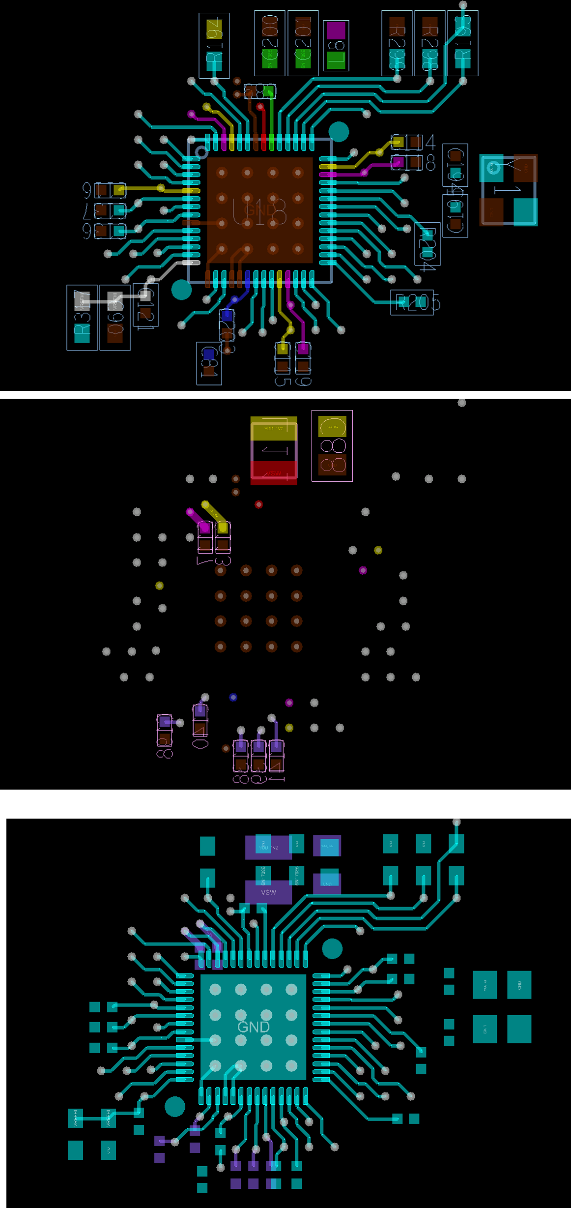
    Here is roughly what I have on the layout so far. First two images are the top and bottom layers, with the important nets color coded as follows:

    Brown is GND.

    Yellow is the 1.2V Vdd

    Pink is the 3.3V Vddio

    Green is the 3.3V for the VDDIO_SW pin (separated from Vddio with ferrite bead L8)

    Red is the switching node VSW

    Blue is Vdda

    White is Vrefhi

    The third image is both layers, but without the nets color coded, just for clarity on how the vias connect. Obviously there's a lot of routing left to do, but the overall strategy is clear.

    I prioritized shrinking the high frequency loop formed by VSS_SW, VDDIO_SW, and a 0402 bypass cap. I connect the VSS_SW pin to an inner GND plane through its own via, rather than connecting directly to the body pad, in order to help restrict that high frequency path. In order to do this, the inductor is on the bottom side and connects to VSW with a via.

    The fact that VSS_SW and VDDIO_SW are on either side of VSW makes this way more difficult than it ought to be, IMO. I can see that the other packages also have the same ordering for these pins. Do you have any reference designs for the 64 or 100 pin packages which make use of the internal DCDC? That might still be helpful here.

    Any feedback would be appreciated.

  • Hi Mike,

    Thank you for providing your layout. On first glance, I do not see any major issues. If you are open to using the other packages as reference, please refer to the TMDSCNCD280049C control card layout, which can be found in C2000Ware. This is our best-designed EVM which provides the most support for the C2000 chip. I will reach out to my colleagues to see if such a specific reference design is available which uses the DC-DC reg. I will get back to you.

    Regards,

    Peter

  • Apologies for the delay. I reached out to another subject matter expert and a reference design tailored specifically for the internal DC-DC regulator is not something that we have. The best bet again is using the layout provided with the controlCARD for reference on what to do with the _SW pins. Please let me know if you were able to examine that layout.

    Regards,

    Peter

  • Hi Peter,

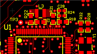
    I did look at the controlCard layout, it does include the DCDC circuitry (though in the schematic it's not actually used due to depopulated resistors). It does put the inductor on the top layer, very close to the chip:

    This is only possible because most of the signals fan out towards the center of the chip. Not possible with the RSH package due to the body pad (unless maybe you use a very fancy HDI process).

    Is it still advisable to put bypass capacitors on the bottom layer with a 0.093" thick stackup?

  • Hi Mike, 

    Yes, you are able to put the bypass capacitors on the bottom layer if you make sure to minimize the trace lengths.

    Having the caps underneath is common in a lot of designs, and is sometimes a necessity when dealing with some BGA packages. What really affects the effectiveness of the bypass cap is the length from the VSS/VDD pins to the pads of the caps. There is not a definitive value that we push for (we just recommend to keep the traces running from the pins to the pads as short as possible) but if I had to put a number on it, I would say that the traces should not exceed a quarter inch including the thickness of the board. From your images, you may need to rework the signal fanout from the pins to prioritize these bypass capacitors. 

    As you can see from the controlCARD layout, it looks like the inductor should be close, but the trace lengths don't matter as much as it does for the bypass caps.

    Regards,
    Peter