


Hi team,
After porting the 28034 LIN-related program to the 280025, it is found that the data is not received, and the 280025 register is basically configured as 28034, and the it can communicate properly on the 28034 board.
The configurations on the 280025 are as follows:
//Pin and Clock Configuration
EALLOW;
CpuSysRegs.PCLKCR19.bit.LIN_A = 1;
GpioCtrlRegs.GPAPUD.bit.GPIO28 = 0; //GPIO28 (LIN TX)
GpioCtrlRegs.GPAPUD.bit.GPIO29 = 0; //GPIO29 (LIN RX)
GpioCtrlRegs.GPAQSEL2.bit.GPIO29 = 3;
GpioCtrlRegs.GPAQSEL2.bit.GPIO29 = 0x01;
GpioCtrlRegs.GPACTRL.bit.QUALPRD3 = 0x03;
GpioCtrlRegs.GPAGMUX2.bit.GPIO28 = 2;
GpioCtrlRegs.GPAMUX2.bit.GPIO28 = 2;
GpioCtrlRegs.GPAGMUX2.bit.GPIO29 = 2;
GpioCtrlRegs.GPAMUX2.bit.GPIO29 = 2;
EDIS;
//LIN register configuration
EALLOW;
LinaRegs.SCIGCR0.bit.RESET = 0;
LinaRegs.SCIGCR0.bit.RESET = 1;
LinaRegs.SCIGCR1.bit.SWnRST = 0;
LinaRegs.SCIPIO0.bit.RXFUNC = 1; //These two sentences are not available on 28034
LinaRegs.SCIPIO0.bit.TXFUNC = 1; //the left configurations are all as same as 28034's
LinaRegs.SCIGCR1.bit.SLEEP = 0;
LinaRegs.SCIFLR.bit.TXWAKE = 0;
LinaRegs.SCIFLR.bit.TXEMPTY = 1;
LinaRegs.SCIFLR.bit.TXRDY = 1;
//Configured as data receive
LinaRegs.SCIGCR1.bit.RXENA = 1;
LinaRegs.SCIGCR1.bit.TXENA = 0;
LinaRegs.SCIGCR1.bit.TIMINGMODE = 1; //Asynchronous Timing
LinaRegs.SCIGCR1.bit.CLK_MASTER = 1; //Enable SCI Clock
LinaRegs.SCIGCR1.bit.CONT = 1; //Continue on Suspend
LinaRegs.SCISETINT.bit.SETRXINT = 1;
LinaRegs.SCISETINT.bit.SETTXINT = 1;
LinaRegs.SCIFORMAT.bit.CHAR = 0x7;
LinaRegs.SCIGCR1.bit.SWnRST = 1;
EDIS;
Data frame sent during debug: 01 03 F0 08 00 01 36 C8
1) when debugging on the board of 28034, checking the configuration of the register is as below:
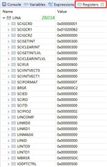
After receiving a frame of data, the result of the receive register is shown in the following figure (RXENA and RXIN are 1 before the data is received):

2) when debugging on the board of 280025, checking the configuration of the register is as below:

While the configuration of the register in Expressions is as below:

RXENA and RXIN both are 0,but in the previous figure, there's a value. Why is that?
3) When transmitting the same data frame as the 28034 test, LinaRegs.SCIRD.bit.RD does not change. The input of GPIO29 is measured when a data frame is sent, as shown in the following figure:

GPIO29 does have data transferred in, but the receive register does not have any value. In combination with the previous register display, does it mean that the register configuration failed?
And from the block diagram of the LIN structure in the data manual, as long as RXENA is configured to 1, SCIRD should be able to receive data, is that right? However, different results are seen through Expressions and Registers.
Could you help check this case? Thanks.
Best Regards,
Cherry
