


Part Number: TMS320F280039C
Hi Experts,
F290039C is under evaluation on customer side. They are working on the schematic now.
Based on the datasheet of F280039C, there are two parameters need to confirm:
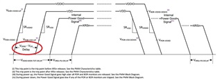
1. For external VREG Power Up sequence, VDDIO should come up first, ad VDD should come up next;
Could you confirm the most suitable delay for those two power? It just show the min value, how about the max value?
2. For the power up SR, VDDIO and VDD need meet 20~100mV/us. It show the faster SR will trigger internal ESD. Could you share the detail information for this?
Otherwise, if the power up SR too slow(< 20mV/us), what's the effect on device?

Best Regards
Songzhen Guo

