This thread has been locked.

If you have a related question, please click the "Ask a related question" button in the top right corner. The newly created question will be automatically linked to this question.

TMS320F280049C: Question about ADC & DAC

Part Number: TMS320F280049C

Dear team:

After configuring the DAC according to the code above, my customer found that after initializing the DAC in the main function, the sampling value of the program will become different from that when the DAC is not used, so it needs to be recalibrated. Moreover, after commenting out the DAC code, the sampling of the system returns to normal. Will DAC affect ADC sampling?

In addition, how to set the maximum output voltage of 280049 DAC to 3.3V?

Best regards

  • Hi,

    DAC output pins are shared with the some of the ADC input pins. Please check the device datasheet for more information on multiplexed pins.

    In addition, how to set the maximum output voltage of 280049 DAC to 3.3V?

    Refer to below table available in device TRM for configuring maximum DAC output. Apart from this, DACVAL should be set to maximum value.

    Thanks
    Vasudha

  • Hi Vasudha:

    The customer has no doubt about pinmux. The problem is that after DAC is enabled, the sampling value of ADC will be too large as a whole, just like the voltage is raised as a whole. After recalibration, the ADC sampling value still has a small difference.

    Best regards

  • Hi,

    after initializing the DAC in the main function, the sampling value of the program will become different from that when the DAC is not used, so it needs to be recalibrated

    Can you provide more details on how the sampling value is being calculated? 

    Thanks
    Vasudha

  • Hi Vasudha:

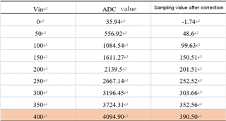
    This is the ADC sampling data after the DAC is turned on:

    As can be seen from the schematic diagram

    when vbulk is 400V, the partial voltage should be 2.597v and the register value of ADC should be 3223. The actual tested register value is 4094.9, which has almost reached the maximum value.

    When vbulk = 300V, the partial voltage should be 1.948v and the DAC value should be 2417. But the experiment shows that the actual ADC value is 3196, and almost all values have been raised.

    Best regards

  • Hi Green,

    Is HV_SENSE going directly to an ADC channel without op amp buffering?  Please note that the voltage divider consisting of R46,48,49 & 51 would form a source resistance of (510K+510K+510K)||10K for an equivalent source resistance of ~9.9K.  On top of this, there is a source capacitance of 1nF.  External RC is too high so this will require a huge SH (not sure if ACQPS register with a max value of 511 can provide the minimum required sample and hold time), but for guidance, please refer to the the section in ADC "Choosing an Acquisition Window Duration" and try to plug in these external RC values to see the minimum SH required for such an external circuit.  To increase the drive strength of the divided signal going into HV_SENSE and isolate the ADC input from the high impedance from the external RC, a strong recommendation is to use a unity gain buffer at HV_SENSE before feeding the signal to the ADC chaannel.

    Now for DAC question:  Once DAC output is enabled, a DAC internal load resistor in the order of a few Kohms will be connected.  This would further complicate the input impedances that the ADC will see.  If unbuffered, the internal DAC load would be another source of input impedance and the effect of this is that the ADC sampling capacitor will never have the chance to settle to its stable value since minimum SH time as discussed in section "Choosing an Acquisition Window Duration" would change.

    Regards,

    Joseph