Part Number: TMS320F28388D
Other Parts Discussed in Thread: C2000WARE
We have a custom board with two TMS320F28388D processors on it. I've been able to connect to the processors and run and debug small applications running from RAM fine. Our program has grown to be bigger than the allotted space for RAM, so now I'm trying to figure out how to run the application from flash.
I have a blinky project that is very small and can run from RAM, but as soon as I run it from flash I run into issues.
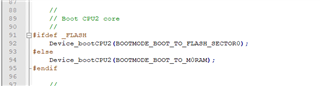
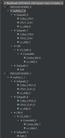
The same project loaded to flash on the first processor in the JTAG chain can run/debug fine from both RAM and flash. The second can only debug from RAM. I can flash it fine (the LED starts blinking on powerup) by launching the target config below,
Connect Target

Load the program. I then get the following debug output
C28xx_CPU1_0: GEL Output:
Memory Map Initialization Complete
C28xx_CPU1_0: GEL Output:
... DCSM Initialization Start ...
C28xx_CPU1_0: GEL Output:
... DCSM Initialization Done ...
C28xx_CPU1_0: GEL Output:
 CPU2 is out of reset and configured to wait boot.
 (If you connected previously, may have to resume CPU2 to reach wait boot loop.)
C28xx_CPU1_0: GEL Output:
 CM is out of reset and configured to wait boot.
 (If you connected previously, may have to resume CM to reach wait boot loop.)
C28xx_CPU1_0: If erase/program (E/P) operation is being done on one core, the other core should not execute from shared-RAM (SR) as they are used for the E/P code. User code execution from SR could commence after both flash banks are programmed.
C28xx_CPU1_0: Only CPU1 on-chip Flash Plugin can configure clock for CPU1, CPU2 and CM Flash operations. Plugin automatically configures PLL when CPU1 Flash operations are invoked. However, if users want to do only CPU2 or CM Flash operations without doing a prior CPU1 operation in the current session, they should click on 'Configure Clock' button in CPU1's on-chip Flash Plugin before invoking CPU2 and CM Flash operations. When this button is used, Flash Plugin will configure the clock for CPU1/CPU2 at 190MHz and CM at 95MHz using INTOSC2 as the clock source. Plugin will leave PLL config like this and user application should configure the PLL as required by application.
C28xx_CPU1_0: GEL Output:
... DCSM Initialization Start ...
C28xx_CPU1_0: GEL Output:
... DCSM Initialization Done ...
C28xx_CPU1_0: GEL Output:
 CPU2 is out of reset and configured to wait boot.
 (If you connected previously, may have to resume CPU2 to reach wait boot loop.)
C28xx_CPU1_0: GEL Output:
 CM is out of reset and configured to wait boot.
 (If you connected previously, may have to resume CM to reach wait boot loop.)
C28xx_CPU1_0: Writing Flash @ Address 0x00080000 of Length 0x00000002 (page 0)
C28xx_CPU1_0: GEL Output:
... DCSM Initialization Start ...
C28xx_CPU1_0: GEL Output:
... DCSM Initialization Done ...
C28xx_CPU1_0: GEL Output:
 CPU2 is out of reset and configured to wait boot.
 (If you connected previously, may have to resume CPU2 to reach wait boot loop.)
C28xx_CPU1_0: GEL Output:
 CM is out of reset and configured to wait boot.
 (If you connected previously, may have to resume CM to reach wait boot loop.)
C28xx_CPU1_0: PLL configuration status = 1. PLL configured successfully.
C28xx_CPU1_0: Erasing Flash Bank 0, Sector 0
C28xx_CPU1_0: Erasing Flash Bank 0, Sector 1
C28xx_CPU1_0: Erasing Flash Bank 0, Sector 2
C28xx_CPU1_0: Erasing Flash Bank 0, Sector 3
C28xx_CPU1_0: Erasing Flash Bank 0, Sector 4
C28xx_CPU1_0: Erasing Flash Bank 0, Sector 5
C28xx_CPU1_0: Erasing Flash Bank 0, Sector 6
C28xx_CPU1_0: Erasing Flash Bank 0, Sector 7
C28xx_CPU1_0: Erasing Flash Bank 0, Sector 8
C28xx_CPU1_0: Erasing Flash Bank 0, Sector 9
C28xx_CPU1_0: Erasing Flash Bank 0, Sector 10
C28xx_CPU1_0: Erasing Flash Bank 0, Sector 11
C28xx_CPU1_0: Erasing Flash Bank 0, Sector 12
C28xx_CPU1_0: Erasing Flash Bank 0, Sector 13
C28xx_CPU1_0: Data has been buffered at the end of the current data block for 64-bit aligned writes.
C28xx_CPU1_0: Writing Flash @ Address 0x00082000 of Length 0x00000fdf (page 0)
C28xx_CPU1_0: Data has been buffered at the end of the current data block for 64-bit aligned writes.
C28xx_CPU1_0: --Verifying Flash @ Address 0x00082000 of Length 0x00000FDC
C28xx_CPU1_0: Writing Flash @ Address 0x00086000 of Length 0x0000012d (page 0)
C28xx_CPU1_0: Data has been buffered at the end of the current data block for 64-bit aligned writes.
C28xx_CPU1_0: --Verifying Flash @ Address 0x00086000 of Length 0x0000012C
C28xx_CPU1_0: Writing Flash @ Address 0x00088000 of Length 0x00000014 (page 0)
C28xx_CPU1_0: --Verifying Flash @ Address 0x00088000 of Length 0x00000014
C28xx_CPU1_0: Writing Flash @ Address 0x00090000 of Length 0x000002f5 (page 0)
C28xx_CPU1_0: Data has been buffered at the end of the current data block for 64-bit aligned writes.
C28xx_CPU1_0: --Verifying Flash @ Address 0x00090000 of Length 0x000002F4
C28xx_CPU1_0: Writing buffered data @ Address 0x00080000 of Length 0x00000004
C28xx_CPU1_0: --Verifying Flash @ Address 0x00080000 of Length 0x00000004
C28xx_CPU1_0: Writing buffered data @ Address 0x00082FDC of Length 0x00000004
C28xx_CPU1_0: --Verifying Flash @ Address 0x00082FDC of Length 0x00000004
C28xx_CPU1_0: Writing buffered data @ Address 0x0008612C of Length 0x00000004
C28xx_CPU1_0: --Verifying Flash @ Address 0x0008612C of Length 0x00000004
C28xx_CPU1_0: Writing buffered data @ Address 0x000902F4 of Length 0x00000004
C28xx_CPU1_0: --Verifying Flash @ Address 0x000902F4 of Length 0x00000004
C28xx_CPU1_0: Trouble Setting Breakpoint with the Action "Finish Auto Run" at 0x82ed4: (Error -1066 @ 0x82ED4) Unable to set/clear requested breakpoint. Verify that the breakpoint address is in valid memory. (Emulation package 9.6.0.00172)
The last part is then where I remain stuck. Is there somewhere where you need to specify the start position or breakpoint address to be different because of the fact that it is on processor 2?
I'm using CCS 11.1.0
Thank you