This thread has been locked.

If you have a related question, please click the "Ask a related question" button in the top right corner. The newly created question will be automatically linked to this question.

TMS320F28379S: unexpected power failure flash procedure

Part Number: TMS320F28379S


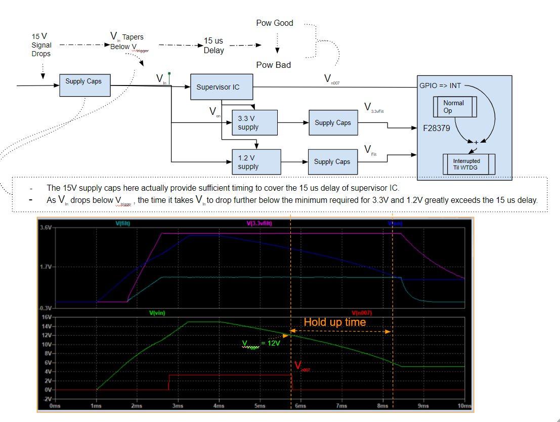
asking for any input regarding any established procedure in the event of an unexpected power failure where some supply capacitance would provide a runtime window before power down of mcu. Specifically for the purpose of executing writes to flash. Also, what would be expected cycle counts per flash word write? What would variance be with and without ecc?

High level is envisioned as

1. GPIO detection of power loss triggers an unmaskable interrupt

2. pre specified volatile memory is written to pre erased nv memory.

I understand this is somewhat generic so any helpful resources is appreciated.

Regards,

Tyler

  • Hi Tyler,

    Typically on an unexpected power failure as long as Flash operation is aborted/suspended/completed before VDDIO and VDD reaches Vmin voltage then Flash will not get corrupted and finish successfully, below Vmin voltages Flash operation is not guaranteed.

    There is no variance w.r.t to ECC bits programming, most of the writes should happen within 1 to 2 pulse counts.

    Are you trying to copy the RAM content into the Flash on a power failure and design a supply cap that can hold the voltage levels for that long until the content is copied?

    It is not recommended because the supply cap may not be able to support transient currents that are needed during Flash programming operation. Flash programming time is specified in the data sheet which you can use for reference.

    Best Regards,

    Nirav

  • Hello Nirav,

    Are you trying to copy the RAM content into the Flash on a power failure and design a supply cap that can hold the voltage levels for that long until the content is copied?

    Yes, this was the idea. 

    It is not recommended because the supply cap may not be able to support transient currents that are needed during Flash programming operation. Flash programming time is specified in the data sheet which you can use for reference.

    Ok, Is there a best practice to stop further transfer? 

    With your above input we are conceiving using an ic to trigger a gpio. This circuit has a 15 ms delay though. So we have supply cap'ed to get passed this delay, then will trigger an interrupt from gpio to stop any further memory transfer/execution. Does this seem reasonable?

    Regards,

    Tyler

  • Hi Tyler,

    How will F28379S know there is a power failure and it needs to start copying the content into Flash during that 15ms delay from external PMIC before the GPIO interrupt comes?

    Best Regards,

    Nirav

  • This is the challenge. We originally thought to use what is called a supervisor IC. But rethinking we realize this is more inline with a battery circuit. 

    can think of it it like this:

    The top drawing is original concept. The bottom is revised concept. We still will be using Supervisor, but this is for power up sequencing and not necessarily pertinent to this issue. Note: input to adc would be safety clamped.

    Input is appreciated.

    Regards,

    Tyler Peterson

  • We realized something we over looked. I think we have resolved issue. However, Any input as to actual implementation in C28379 fw is appreciated

  • I mislabled the signal to gpio in drawing from what is shown in simulation. 
      

  • Hi Tyler,

    Thanks for the details, still I have few questions:

    1. What is V(En) signal is it the output of a LDO, can you add that in your drawings?

    2. What is the trip point of Supervisor IC?

    3. In your simulation what is the voltage on V3.3Vfilt / supply going into F28379S when GPIO trips? Based on your simulation it appears to be still at 3.3V, is that correct?

    4. Can you model your simulation with current load equal to device max current i.e. 400mA on VDD and 30mA on VDDIO?

    Best Regards,

    Nirav

  • 1. What is V(En) signal is it the output of a LDO, can you add that in your drawings?
     Ven is signal to supplies for power up sequence

    2. What is the trip point of Supervisor IC?
    12 V the threshold. 

    3. In your simulation what is the voltage on V3.3Vfilt / supply going into F28379S when GPIO trips?

    3.3V

    Based on your simulation it appears to be still at 3.3V, is that correct?

    yes

    4. Can you model your simulation with current load equal to device max current i.e. 400mA on VDD and 30mA on VDDIO?

    From Colleague:

    ,I have the 400mA and 30mA on the VDD and VDDA, respectively. Also, I have the remaining estimated load (2.5W) on the 15V to make it fall faster. You can see that the 15V begins to fall, and when it crosses 12V, our GPIO should go LOW. It is still falling, but the LM2734s should still be enabled and supporting VDD and VDDA until the Vin reaches ~5V. The LM2734s are disabled and VDD and VDDA quickly fall
    simulation matches my calculation of ~1.8ms between the GPIO going LOW and VDD and VDDA falling
    If you want, I can also tie the enable pin an ADC input so we can measure that

  • Hi Tyler,

    This is good data, as you can see you have only ~2ms time to copy the data from RAM to Flash, if you go through the data sheet you will see the Flash programming operation may take longer, also it depends on how much data you wish to copy into Flash.

    How many words you wish to copy into the Flash on a brown out event?

    Best Regards,

    Nirav