This thread has been locked.

If you have a related question, please click the "Ask a related question" button in the top right corner. The newly created question will be automatically linked to this question.

TMS320F28020: Modifying the Linker Command File to Create a New Memory Map

Part Number: TMS320F28020
Other Parts Discussed in Thread: TMS320F28027

Hi All,

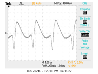
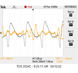
I recently started a project using a LaunchPadXL TMS320F2802x.  I started with an example and added some simple test code to exercise the SCIA and I2C interfaces, one project file at a time.

Now, I have target prototype hardware in-hand that contains a TMS320F28020 MCU.  The memory map of the 28020 is smaller than the LaunchPad's 28027.  So, now when I compile the same code to run in the smaller memory space, I get an error indicating reference to a memory region that doesn't exist, like this:

C28xx: Loader: One or more sections of your program falls into a memory region that is not writable.  These regions will not actually be written to the target.  Check your linker configuration and/or memory map.

I'm having a hard time understanding the different linker command files and other references to memory mapping.

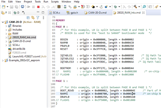
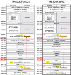
The memory map file generated during the make process shows RAML0 starting at 0x8000 and extending into 0x85ff as follows:

Fullscreen
1
2
3
4
5
6
7
8
9
10
11
12
13
14
MEMORY CONFIGURATION
name origin length used unused attr fill
---------------------- -------- --------- -------- -------- ---- --------
PAGE 0:
BEGIN 00000000 00000002 00000002 00000000 RWIX
RAMM0 00000050 000003b0 000003b0 00000000 RWIX
RAML0 00008000 00000600 00000377 00000289 RWIX
FLASHC 003f2000 00002000 00000000 00002000 RWIX
IQTABLES 003fe000 00000b50 00000000 00000b50 RWIX
IQTABLES2 003feb50 0000008c 00000000 0000008c RWIX
IQTABLES3 003febdc 000000aa 00000000 000000aa RWIX
BOOTROM 003ff27c 00000d44 00000000 00000d44 RWIX
RESET 003fffc0 00000002 00000000 00000002 RWIX
XXXXXXXXXXXXXXXXXXXXXXXXXXXXXXXXXXXXXXXXXXXXXXXXXX

However, the 28020 physical RAML0 memory starts at 0x8000 and only extends to 0x83ff.

At first, I thought this was because the setting in the project >Properties>CCS General Project tab was set to Variant TMS320F28027:

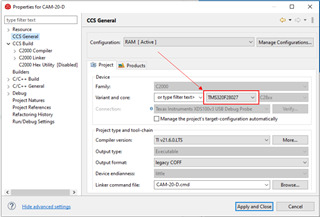
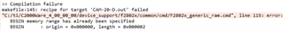
But, when I changed it to 28020, I got multiple duplicate memory range errors:

I will need to manipulate the memory map before the project is done in several ways to fit all the code into available memory.  I could use some help understanding the appropriate ways to modify the memory map.

I have used the linker command file to make minor changes in the past, so I understand that part of it, but I don't know why the linker still thinks RAML0 is the longer than it really is.

Questions:

1. Why does the make file end up with a memory map that includes address space that doesn't exist in the physical part?

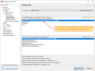
2. Where is it getting the linker command file that tells it each memory's location and size?  The linker command file that was copied into the project folder after changing the Variant setting shows the correct length of RAML0.

3. How do .gel files factor into the equation?

4. Is there an app note describing the memory mapping configuration architecture?  I'm looking for info about manipulating linker cmd files, gel files, properties settings, etc..

Thanks,
robin

  • More info...

    I found where a second linker cmd file is invoked:

    After deleting that entry, I was able to compile/link without the duplication errors.

    I still had memory size issues but was able to modify the linker cmd file and reduce .stack size to get everything to fit and run:

    I would still like to know if there's an app note or design guide that explains the use of gel files, linker command files, how to invoke them, edit them, etc..

    Thanks,
    robin

  • Hi Robin,

    For linker command files, you may refer to the following documents -

    https://software-dl.ti.com/ccs/esd/documents/sdto_cgt_Linker-Command-File-Primer.html

    https://www.ti.com/lit/ug/spru513r/spru513r.pdf (Chapter Linker Description)

    For gel files - 

    https://software-dl.ti.com/ccs/esd/documents/users_guide/ccs_debug-gel.html

    Hope this helps.

    To answer you question on inker command file path, you can either have it as a file added in the CCS project structure or in the --library option in the project properties. Please make sure you use the correct linker command file corresponding to the device part number you use.

    Regards,

    Veena

  • Hi Veena,

    Thanks for the ref materials.  I haven't had a chance to read them but will over the weekend.

    I added some flash memory to the linker command file and moved .cinit from PRAML0 to FLASH0: (ignore comments)

    Fullscreen
    1
    2
    3
    4
    5
    6
    7
    8
    9
    10
    11
    12
    13
    14
    15
    16
    17
    18
    19
    20
    21
    MEMORY
    {
    PAGE 0 : // Program memory space (initialized sections)
    /* For this example, L0 is split between PAGE 0 and PAGE 1 */
    /* BEGIN is used for the "boot to SARAM" bootloader mode */
    BEGIN : origin = 0x000000, length = 0x000002
    RAMM0 : origin = 0x000040, length = 0x0006C0
    PRAML0 : origin = 0x008000, length = 0x000250
    RESET : origin = 0x3FFFC0, length = 0x000002
    IQTABLES : origin = 0x3FE000, length = 0x000B50 /* IQ Math Tables in Boot ROM */
    IQTABLES2 : origin = 0x3FEB50, length = 0x00008C /* IQ Math Tables in Boot ROM */
    IQTABLES3 : origin = 0x3FEBDC, length = 0x0000AA /* IQ Math Tables in Boot ROM */
    BOOTROM : origin = 0x3FF27C, length = 0x000D44
    // RAMM1 : origin = 0x000400, length = 0x000200 /* on-chip RAM block M1 */
    FLASH0 : origin = 0x3f4000, length = 0x001000
    PAGE 1 : // Data memory (UNinitialized sections)
    XXXXXXXXXXXXXXXXXXXXXXXXXXXXXXXXXXXXXXXXXXXXXXXXXX

    With .cinit assigned to PRAML0, the code runs on the target.  With .cinit assigned to FLASH0, the project compiles and builds without error, but while uploading to target (after erasing flash and while trying to upload .cinit), I get error - 1156:

    If I click "No" the following "Load program Error" pops up:

    After that, upon another attempt to compile/build, I get error - 233:

    At this point, the target board appears to be bricked.  I'm not able to connect to it at all.  I've tried different cables, different XDS100 interface, different computer, and all fail to connect.  A fresh target board connects without issue.

    This has happened twice.  The first time I reassigned .text to FLASH0.  When it first happened with the first target board, I selected "Yes" in the Error - 1156 dialog.  That didn't allow connection, but it didn't brick the target either.  I only have one more prototype of the target board, so must proceed very cautiously.

    Do you see where the problem lies?  Any ideas?  Is there any way to recover the target board without replacing the TMS320F28020?

    I'm afraid to continue until this is worked out.  I don't want to risk destroying my last proto board.

    Thanks,
    robin

  • Hi Robin,

    I will loop in the Flash expert to help you better/

    Regards,

    Veena

  • Robin,

    From the error message and the after effects I think there may have been a reset event during the programming, which in turn corrupted the CSM password stored in flash at 0x3F7FF8-3F7FFF.

    For the devices that will no longer connect, if you change the boot mode to wait boot mode, this should allow you to connect the device to CCS

    Once connected open up a memory window to the password addresses mentioned above, and see if you read back 0x0000.  If you see 0x0000, then the password is programmed to something indeterminate and the device is not salvageable.  If  you see anything else then the CSM is not programmed and we can look into that scenario(I'm going to assume it will be 0x0000 on the bad devices for the below).

    I'd like to first check that there is/was adequate supply current for the flash erase/program cycle:  below is from page 33 of the DS https://www.ti.com/lit/ds/symlink/tms320f28027.pdf

    If there was inadequate supply it could result in a droop in the VDDIO supply(assuming you are using the on-chip VREG) which would activate the internal Brown Out Reset, interrupting the flash operation and resulting in non 0xFFFF values in the password locations.  In addition to the supply being capable of the above, we should also look at the relative location of the decaps on the VDDIO pin to make sure they are close to the device and of the correct value(I believe we use a 2.2uF cap on the LaunchPad).

    In terms of debugging this functionally it will be a safer option to only use sectors B and/or C for now(on the good device) as there is less chance of effecting the passwords if there is an event.  You would also want to change the settings in the Flash tools in CCS to not erase sectors A/D if you decide to program the good unit while we figure this out.  By default any flash programming operation will erase all sectors even if there is not a need to do so from a the .coff POV.

    Will look for your findings on the above and we can go from there.

    Best,
    Matthew

  • Hi Matthew,

    Thanks for your response.

    Boot mode was wired for "GetMode", but now I've reconfigured it to 'Wait' boot mode.  I did that by pulling GPIO34 low.  /TRST was already pulled low, and TDO was already pulled high.  Now, when I open the memory browser to 0x3f7ff8, here's what I see:

    Clearly, the CSM password has been set to non-0xffff values.  I'll have to replace the part on the two boards that this happened to.

    Now the big question, "How did it happen?"

    My target module is being powered vie PoE with a power rating of 30W.  I'm not sure if those are real or marketing Watts, and I don't see published spec's to find out.  I imagine it's providing around 25-50V at between 0.5 and 1.0A.  I have a 1.0A/5V LDO feeding a 500mA/3.3V LDO regulator on my target board.  I've watched the power supply line during flash erases and don't see it falling anywhere near 5%.  It looks pretty stable.  I've also programmed the target dozens of times without any issue, before adding FLASH0 to the linker command file.  I added FLASH0 and reprogrammed many times without issue.  It was only when I tried linking either .cinit or .text to FLASH0 that the problem occurred.

    Vddio pins have 1.2uF caps close to the part's pins, as recommended on page 12 of the datasheet you mention above.

    The code started life using a LaunchXL TMS320F28027, which has more onboard flash.  If a gel file or linker command file was still set up for the 28027 when I flashed the 28020, that might explain it.  BUT, as far as I know the gel and linker command files have been correct for the 28020.

    Thoughts?

    Thanks,
    robin

  • Robin,

    Thanks for the additional info, from what you've said I also doubt that the supply is an issue. 

    Inside of CCS, after you have launched the target config, click on "Tools"->"On-Chip Flash" and compare the window to the below.  This is what CCS will use when you "load" a coff file that includes mapped flash addresses.  Note the sector sizes, as these will be what is different from a 28020 vs 28027.  CCS should give a warning, however, if the 28027 sizes(2x more) were in place for a 28020 target.

    Please also confirm that the Key0-7 are showing all FFFF.

    The above settings is what I was referring to if we want to avoid erasing those sectors that are unused by your project.

    Once we decide to attempt to program another device,we can consider un-checking erase on A/D as well as re-mapping your FLASH_H0 to sector B or C to be conservative until we are sure of the root cause.  A mis-programmation of B/C should not result in a locked device.

    Your linker is correct for the 28020 device.  Can you look in the debug directory of your project and also send back the *.map file?  I can review this to confirm that sector D is all that is being loaded.

    Finally, from the above comment on voltage rail goodness, I assume you are using the on-chip VREG.  Please check to see that pin VREGENZ is hard tied to VSS(correct) vs a pulldown resistor(incorrect).

    Best,
    Matthew

  • Hi Matthew,

    My On-Chip Flash configuration matches your image above.  Here's an image of my window:

    After the load error, I switched the comments such that .cinit was no longer assigned to FLASH0 and was reassigned to PRAML0, then recompiled.  As a result, the .map file from that day shows .cinit loaded in PRAML0.

    Since the .map file from that day doesn't reflect the memory configuration that caused the problem, today I switched the comments back, to put .cinit in FLASH0.  Then rebuilt the project to produce a .map file that was what would have been in place when the load error occurred.

    I renamed each .map file accordingly and have attached them both:

    1. CAM-20-D_PRAML0.map

    Fullscreen
    1
    2
    3
    4
    5
    6
    7
    8
    9
    10
    11
    12
    13
    14
    15
    16
    17
    18
    19
    20
    21
    ******************************************************************************
    TMS320C2000 Linker PC v21.6.0
    ******************************************************************************
    >> Linked Fri Apr 1 12:19:43 2022
    OUTPUT FILE NAME: <CAM-20-D.out>
    ENTRY POINT SYMBOL: "code_start" address: 00000000
    MEMORY CONFIGURATION
    name origin length used unused attr fill
    ---------------------- -------- --------- -------- -------- ---- --------
    PAGE 0:
    BEGIN 00000000 00000002 00000002 00000000 RWIX
    RAMM0 00000040 000006c0 000005dc 000000e4 RWIX
    PRAML0 00008000 00000250 000000c5 0000018b RWIX
    FLASH0 003f4000 00001000 00000000 00001000 RWIX
    IQTABLES 003fe000 00000b50 00000000 00000b50 RWIX
    IQTABLES2 003feb50 0000008c 00000000 0000008c RWIX
    IQTABLES3 003febdc 000000aa 00000000 000000aa RWIX
    XXXXXXXXXXXXXXXXXXXXXXXXXXXXXXXXXXXXXXXXXXXXXXXXXX

    2. CAM-20-D_FLASH0.map

    Fullscreen
    1
    2
    3
    4
    5
    6
    7
    8
    9
    10
    11
    12
    13
    14
    15
    16
    17
    18
    19
    20
    21
    ******************************************************************************
    TMS320C2000 Linker PC v21.6.0
    ******************************************************************************
    >> Linked Mon Apr 11 09:08:45 2022
    OUTPUT FILE NAME: <CAM-20-D.out>
    ENTRY POINT SYMBOL: "code_start" address: 00000000
    MEMORY CONFIGURATION
    name origin length used unused attr fill
    ---------------------- -------- --------- -------- -------- ---- --------
    PAGE 0:
    BEGIN 00000000 00000002 00000002 00000000 RWIX
    RAMM0 00000040 000006c0 000005dc 000000e4 RWIX
    PRAML0 00008000 00000250 00000000 00000250 RWIX
    FLASH0 003f4000 00001000 000000c5 00000f3b RWIX
    IQTABLES 003fe000 00000b50 00000000 00000b50 RWIX
    IQTABLES2 003feb50 0000008c 00000000 0000008c RWIX
    IQTABLES3 003febdc 000000aa 00000000 000000aa RWIX
    XXXXXXXXXXXXXXXXXXXXXXXXXXXXXXXXXXXXXXXXXXXXXXXXXX

    The reason I used On-Chip Flash Sector D to define FLASH0 (e.g., FLASH0 : origin = 0x3f4000, length = 0x001000), was specifically to avoid the CSM addresses (0x3f7ff8 + 8).  I'm happy to try a version using flash sector B or C, but I'm not sure that will circumvent whatever is causing the problem.

    Here's a visual aid I created when migrating from 28027 to 28020:

    Yes, VREGENZ is hard tied to digital ground:

    Do you think it's worth trying to run Depletion Recovery?

    I hope you can find something amiss, because I'm just not seeing it.

    Thanks for your help!
    robin

  • Robin,

    You can try Depletion Recovery on the locked devices, it won't hurt but I don't think it will resolved the locked state.

    Looking at the map file things look good there as well, and even the use of Sector D isn't very big and doesn't run into what would be equivalent addresses of the CSM in Sector A.

    Can you give some more details on the connection between GPIO34 and XRSn?  I know its a bit of a stretch, but we have to make sure that XRSn isn't pulled during the programmation process.  From Reset GPIO34 would be configured as an input, so it shouldn't even be possible for it to drive XRSn until your code runs.  Could you try the RAM only version of your code and note when this pulls XRSn? 

    Based on the MUX function, I would guess you might be using the COMP2 out to trip reset based on a comparator trip, but will let you fill in the details. 

    The interesting thing about this setup is that if you were actively debugging(TRSTn is high), even if XRSn is pulled low you might not see an effect depending on what your code is doing.  But if this activated while programming the flash it could cause some unusual behavior.

    Best,

    Matthew

  • Hi Matthew,

    I was unable to run Depletion Recovery, because it requires the target to be connected.  Since it won't connect, there's no option for Depletion Recovery.

    The connection between GPIO34 and XRSn was carried over from the legacy 8051 version of this product.  It's not needed in this design and I'll remove R11 to break the link.  Anyway, there's no code that controls GPIO34. 

    Here's what happens at GPIO34:

    Power On:
         GPIO34 toggles low for 60us, every 13.5ms.  I don't know why it's doing this.  I'm not sure what's residing in nonvolatile memory at this point.

    Connect Target:
         GPIO34 goes high and stays high.

    Load Program:
         GPIO34 stays high up to and including when it breaks at main().

    Run Program:
         GPIO34 stays high.  There's no code to take it low.

    NEW INFORMATION:

    Upon closer examination, there's quite a bit of noise on the Vddio pin:

    I see a couple of alarming details on the schematic:

    1. The decoupling cap on Vddio is only 0.1uF  on the target board (it's 2.2uF on LaunchXL)

    2. The inductor feeding Vddio is the wrong value.  I specified Abracon P/N: ACML-0603H-600 (60 Ohms at 100MHz, 0.04 Ohms dc, 2.5A), but what got placed on the PCB was an Abracon P/N: ACML-0603H-221 (220 Ohms at 100MHz, 0.1 Ohm dc, 1.4A)

    I don't have the correct inductor, but I added two more of the wrong part in parallel with the existing one, and changed the decoupling cap to 1.2uF.

    Now the power supply rail looks like this: (Yellow trace)

    The negative going excursions are 50% better.  Perhaps with the appropriate inductor they would improve further?

    Vddio has a nominal value of 3.3Vdc.

    As an experiment, I could also short out the inductor to get a much cleaner looking DC on Vddio.

    Is this enough of a smoking gun to make it worth risking my last working prototype?

    Thoughts?

    Thanks,
    robin

  • Robin,

    Good catch on both the decap and the inductor/bead.  If I'm reading the new waveform correctly are we 3.3V +/- 0.192V with the new setup?  This is within the tolerance allowed on VDDIO (3.3V +/-10%)so we should be OK.  With the other waveform, I think it is likely we were tripping the BOR(Brown Out Reset) on the VDDIO rail, especially when the flash is being programmed.

    For the GPIO34 when connected to the XRSn, what you are seeing on power up is the watchdog Reset from the device until you gain control with the debugger.  Since you don't configure GPIO34 it will be an input always, so likely this wasn't doing anything bad to the XRSn pin, but good to get it out of the equation.

    I think you can flash the device, but I would switch to sector B or C, and uncheck A/D in the flash configs for automatic erase just to err on the side of caution.

    Best,

    Matthew

  • Thanks Matthew,

    Vddio noise is about 540mVp-p riding on 3.3Vdc.  At its lowest point, it reaches down to 3.06V, which is still within the 10% tolerance.  Although, the documentation says that BOR tolerance is 5% when the on-board Vreg is enabled.

    I switched my FLASH0 assignment to sector 'C' (FLASH0 : origin = 0x3f5000, length = 0x001000), and assigned .cinit to it. (.cinit : > FLASH0, PAGE = 0).

    Cleaned the project, built it, loaded it, and ran it without issue.

    Feeling a greater degree of confidence, I reassigned .text to FLASH0, and it runs as well.

    So, in a nutshell, I had a problem reassigning sections to flash memory.  At first glimpse, the power supply didn't seem to be a strong suspect.  Upon closer examination, noise on the Vddio pin was dipping below the tolerance allowed on the TMS320F28020, most likely causing a brown-out reset.  No reset occurred during normal operation, but I suspect the current it takes to perform a flash write would increase the noise to a problematic level.  After correcting PCB design flaws where the inductor feeding Vddio and the capacitor decoupling it were wrong values, my program now runs from flash memory.

    Shortly after this success, more power supply problems occurred.  I replaced the two locked MCUs, but at this point all three target proto boards are bricked.  The 3.3V reg is being pulled into overcurrent shutdown by the MCU.  I haven't found the culprit yet, but will start a new thread more appropriate to this issue.

    Thank you Matthew for all your help.  You are a scholar and a gentleman.