


Hello everyone,
I have some problems on the reception of SPI frames in TMS320F28335PGFA, using the McBSP-B as master. I am using the MCP2518FDT CAN controller to add some CAN functionallity through McBSP-B as SPI interface.
I can send a READ frame of 1 phase, 1 word and 32 bits to the MCP2518FDT and it answers as it is shown in the osciloscope image below.
- Blue signal: CLK, MCLKXB
- Yellow signal: SDI, MDXB
- Pink signal: SDO, MDRB

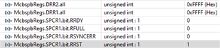
But then if I read the DRR 1 and 2 registers they always show the same, 0xFFFF in CCS and no problems shown.
The McBSP configuration is based on the mcbsp_spi_loopback example (which works correclty for me with de DLB enabled), slightly modified for the MCP2518FDT CAN Controller (CLKSTP=3), shown in the following code snippet:
void InitMcbspb(void)
{
    // McBSP-B register settings
    SysCtrlRegs.PCLKCR0.bit.MCBSPBENCLK = 1; // Enable low speed clk to McBSP-B

    McbspbRegs.SPCR2.all=0x0000;		// Reset FS generator, sample rate generator & transmitter
	McbspbRegs.SPCR1.all=0x0000;		// Reset Receiver, Right justify word
	McbspbRegs.SPCR1.bit.DLB = 0;       // Enable loopback mode for test. Comment out for normal McBSP transfer mode.

	McbspbRegs.MFFINT.all=0x0;			// Disable all interrupts

    McbspbRegs.RCR2.all=0x0;			// Single-phase frame, 1 word/frame, No companding	(Receive)
    McbspbRegs.RCR1.all=0x0;

    McbspbRegs.XCR2.all=0x0;			// Single-phase frame, 1 word/frame, No companding	(Transmit)
    McbspbRegs.XCR1.all=0x0;

    McbspbRegs.SPCR1.bit.CLKSTP = 3; // Clock Stop Mode: Together with CLKXP/CLKRP determines clocking scheme
    McbspbRegs.PCR.bit.CLKXP = 0;    // CLKX Send Polarity: CPOL = 1, CPHA = 0 rising edge no delay
    McbspbRegs.PCR.bit.CLKRP = 0;    // MCLKX Receive Polarity: CPOL = 0, CPHA = 0 rising edge no delay

    //Receiver config
    McbspbRegs.RCR2.bit.RFIG=0;         // Receive  frame sync ignore
    McbspbRegs.RCR2.bit.RCOMPAND=0;     // Receive  Companding Mode selects
    McbspbRegs.RCR2.bit.RPHASE=0;       // Receive Phase
    McbspbRegs.XCR2.bit.XPHASE=0;       // Transmit Phase

    McbspbRegs.XCR2.bit.XDATDLY=01;     // Transmit data delay bits.  1: 1-bit data delay
    McbspbRegs.RCR2.bit.RDATDLY=01;     // Receive data delay bits.   1: 1-bit data delay

    InitMcbspb32bit();                  // 7:5    Receive and Send  word length

    McbspbRegs.RCR1.bit.RFRLEN1=0;      // In SPI mode must be 0. Number of words per phase 1
    McbspbRegs.XCR1.bit.XFRLEN1=0;      // In SPI mode must be 0. Number of words per phase 1

    // CLK config
    McbspbRegs.SRGR2.bit.CLKSM = 1;		// CLKSM=1 (If SCLKME=0, i/p clock to SRG is LSPCLK)
	McbspbRegs.SRGR2.bit.FPER = 1;		// FPER = 1 CLKG periods
	McbspbRegs.SRGR2.bit.FSGM = 0;
    McbspbRegs.SRGR1.bit.FWID = 1;              // Frame Width = 1 CLKG period
    McbspbRegs.SRGR1.bit.CLKGDV = CLKGDV_VAL;	// CLKGDV_VAL=16 CLKG frequency = LSPCLK/(CLKGDV+1)

    McbspbRegs.PCR.bit.SCLKME = 0;      // Sample rate generator input clock mode bit
   	McbspbRegs.PCR.bit.FSXM = 1;		// Transmit Frame Synchronization Mode
   	McbspbRegs.PCR.bit.FSRM = 1;        // Receive Frame Synchronization Mode
   	McbspbRegs.PCR.bit.CLKXM = 1;		// CLKX generated internally, CLKR derived from an external source
	McbspbRegs.PCR.bit.CLKRM = 1;       // Receiver clock mode CLKRM=1
	McbspbRegs.PCR.bit.FSXP = 1;        // Transmit Frame synchronization polarity FSXP = 1
	McbspbRegs.PCR.bit.FSRP = 0;        // Receive Frame synchronization polarity FSRP = 1

	delay_loop();                // Wait at least 2 SRG clock cycles
    McbspbRegs.SPCR2.bit.GRST=1; // Enable the sample rate generator
	clkg_delay_loop();           // Wait at least 2 CLKG cycles
	McbspbRegs.SPCR2.bit.XRST=1; // Release TX from Reset
	McbspbRegs.SPCR1.bit.RRST=1; // Release RX from Reset
    McbspbRegs.SPCR2.bit.FRST=1; // Frame Sync Generator reset
}
The GPIO pins (24, 25, 26 and 27) are also configured to work as McBSP mode and I transfer the data as:
void MCBSP_B_TransferData(uint16_t *SpiTxData, uint16_t *SpiRxData)
{
    // Transmit 31 - 0 bit data
    while(McbspbRegs.SPCR2.bit.XRDY == 0) {}

           McbspbRegs.DXR2.all= SpiTxData[1];          // 31-16

           McbspbRegs.DXR1.all= SpiTxData[0];          // 15-0

    // Receive 31 - 0 bit data
    while(McbspbRegs.SPCR1.bit.RRDY == 0) {}

        SpiRxData[1]= McbspbRegs.DRR2.all;             // 31-16

        SpiRxData[0]= McbspbRegs.DRR1.all;             // 15-0

}
Maybe is something I have configuring wrong in the reception? Is it possible that the content of DRR2 (0xFFFF) is also buffered into DRR1?
Thank you in advance for the support!
JC


