


Part Number: TMS320F28034
Hello,
I need some help in the design of the hardware interface between the XDS110 debug probe and the TMS320F28034PNS microcontroller that I'm using in my target board.
The target is being powered externally so I don't need the debug probe to power the target. Do I still need the auxiliary interface or just the JTAG interface with the CTI-20 connector?
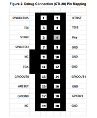
Figure 2 from the user guide shows the pin mapping of the debug connection. I need some help with the connection to the TMS320F28034PNS pins. Pins 1 (TMS), 2 (NTRST), 3 (TDI), 7 (TDO) and 11 (TCK) of the debug cable will be connected to pins 60, 10, 59, 58, 57 of the TMS320F28034PNS. Then, pin 5 (VTRef) will be connected to the 3.3V power supply of the target, pins 9 and 19 (NC) will remain floating and pins 8, 10, 12, 16 and 20 will be connected to the ground of the target. I think these connections are quite straight forward but could you please confirm that they are correct?
Could you then please help me understanding where I should connect pins 4 (TDIS), 6 (Key), 13 (GPIOOUT0), 14 (GPIOOUT1), 15 (nRESET), 17 (GPIOIN0) and 18 (GPIOIN1)?
Thanks
Giorgio


