


Part Number: TMS320F280041
Hello,
I am writing an application requiring low power mode. In the image below from the TMS320F28004x Datasheet, it is advertised that when using DC-DC in Halt mode I should "typically" see 1.7 + 0.2 ~ 1.9mA on the 3V3 line feeding Vddio and Vdda. I am, however, seeing more like 14mA. I am disabling flash and PLL, but I am still seeing these results. Could you please advise?
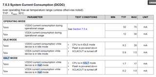
Listed below is my low power mode function running from RAM.
#pragma CODE_SECTION(lpm_enterLowPowerMode, "ramfuncs");
void lpm_enterLowPowerMode(void)
{
    /*      Unlock locked registers     */
    EALLOW;

    /*      Check the arguments.        */
    ASSERT(Flash_isCtrlBaseValid(FLASH0CTRL_BASE));

    /*       Write the power mode to the appropriate register.      */
    HWREG(FLASH0CTRL_BASE + FLASH_O_FBFALLBACK) = (HWREG(FLASH0CTRL_BASE + FLASH_O_FBFALLBACK) & ~((FLASH_FBFALLBACK_BNKPWR0_M) << ((uint32_t) FLASH_BANK0 * 2U))) | ((uint32_t) FLASH_BANK_PWR_SLEEP << ((uint32_t) FLASH_BANK0 * 2U));

    /*      Write the power mode to the appropriate register.       */
    HWREG(FLASH0CTRL_BASE + FLASH_O_FBFALLBACK) = (HWREG(FLASH0CTRL_BASE + FLASH_O_FBFALLBACK) & ~((FLASH_FBFALLBACK_BNKPWR0_M) << ((uint32_t) FLASH_BANK1 * 2U))) | ((uint32_t) FLASH_BANK_PWR_SLEEP << ((uint32_t) FLASH_BANK1 * 2U));

    /*      Write the power mode to the appropriate register.       */
    HWREG(FLASH0CTRL_BASE + FLASH_O_FPAC1) = (HWREG(FLASH0CTRL_BASE + FLASH_O_FPAC1) & ~(uint32_t) FLASH_FPAC1_PMPPWR) | (uint32_t) FLASH_PUMP_PWR_SLEEP;

    /*      Set Idle to Halt        */
    HWREG(CPUSYS_BASE + SYSCTL_O_LPMCR) = (HWREG(CPUSYS_BASE + SYSCTL_O_LPMCR) & ~(uint32_t) SYSCTL_LPMCR_LPM_M) | SYSCTL_LPM_HALT;


    /*      Disable PLL     */
    HWREGH(CLKCFG_BASE + SYSCTL_O_SYSPLLCTL1) &= ~(SYSCTL_SYSPLLCTL1_PLLCLKEN | SYSCTL_SYSPLLCTL1_PLLEN);

    /*      Enter Halt Mode     */
    IDLE;

    /*      Power Up Flash         */
    /*       Write the power mode to the appropriate register.      */
    HWREG(FLASH0CTRL_BASE + FLASH_O_FBFALLBACK) = (HWREG(FLASH0CTRL_BASE + FLASH_O_FBFALLBACK) & ~((FLASH_FBFALLBACK_BNKPWR0_M) << ((uint32_t) FLASH_BANK0 * 2U))) | ((uint32_t) FLASH_BANK_PWR_ACTIVE << ((uint32_t) FLASH_BANK0 * 2U));

    /*      Write the power mode to the appropriate register.       */
    HWREG(FLASH0CTRL_BASE + FLASH_O_FBFALLBACK) = (HWREG(FLASH0CTRL_BASE + FLASH_O_FBFALLBACK) & ~((FLASH_FBFALLBACK_BNKPWR0_M) << ((uint32_t) FLASH_BANK1 * 2U))) | ((uint32_t) FLASH_BANK_PWR_ACTIVE << ((uint32_t) FLASH_BANK1 * 2U));

    /*      Write the power mode to the appropriate register.       */
    HWREG(FLASH0CTRL_BASE + FLASH_O_FPAC1) = (HWREG(FLASH0CTRL_BASE + FLASH_O_FPAC1) & ~(uint32_t) FLASH_FPAC1_PMPPWR) | (uint32_t) FLASH_PUMP_PWR_ACTIVE;

    EDIS;
}

