Hi champs,
My customer is using 176-PIN F28377S and wants to know more about the PowerPAD layout, please advise your comments on below questions,
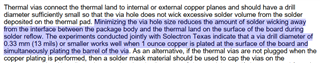
- In datasheet we suggest 0.2 mm diameter via and Application Report slma002h suggests 0.33 mm diameter via, which suggestion is better?
- On the back of PowerPAD, what method is recommended to get better heat dissipation? Is there any risk if customer uses bare copper like the front of PowerPAD?
Regards,
Luke