This thread has been locked.

If you have a related question, please click the "Ask a related question" button in the top right corner. The newly created question will be automatically linked to this question.

TMS320F280025: MCU reset during 2.2KV differential mode surge test

Part Number: TMS320F280025


Hi Champs, 

Customer migrates their digital power supply platform from NXP's DSPs to F280023(PFC) and F280025(LLC).

The firmware is almost done and the unit passed almost all the DVT functional tests, but they're encountering some problem with the surge test.

The primary DSP resets durng 2.2KV differential mode surge test.


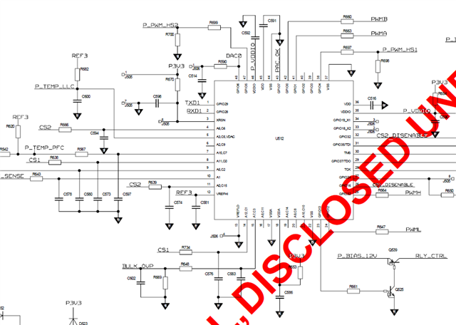
- The main board is using the old main board with the old NXP platform, which had passed surge tests. The control board is redesigned, the aux power is located on the control board.

- They use

- 4K7 pullup to XRNS pin, and use 10nF bypass cap, changing the bypass to 100nF no help.

- 2.2uF cap for each VDDIO pin.

- 10uF cap for each VDD pins.

Please kindly share how to debug and solve this kind of issue. 

Thanks

Tamas

  • It is extremely difficult to debug EMI related issues without access to the schematics, PCB layout and the hardware itself. In other words, remote debug is not practical. Besides, more often than not, finding a solution is an iterative process. The first task is to find whether the noise is coupled conductively or radiatively into the system. i.e. whether the issue at hand is one of conducted immunity or radiated immunity. Once this is identified, we need to identify the entry point of the noise into the system. Only then can we come with a solution. Problem could be related to insufficient decoupling/filtering, incorrect layout, improper (or lack of) shielding etc. There are numerous resources online that deal with this. Hard to explain them in a post. 

    ESD/EMI events are capable of inducing all sorts of bizarre behavior in the device. The solution lies in beefing up the circuit design to make it immune to the disturbance.. Unfortunately, often times, the shortcomings are discovered after the board is made and hence make the redesign of the board necessary.

    Many books have been written on this topic and many papers published. The actual circuit design, the components used, the geometry of the components, the board layout, the board stack-up, the shielding employed , all play a role in the immunity strength of the design.

    You could run your system with INTOSC and see if it gets affected. If not, noise may be coupling through the crystal oscillator circuitry. It is conceivable the missing-clock-circuitry kicks in. You have not mentioned about how your system handles a missing clock.

    - 4K7 pullup to XRNS pin, and use 10nF bypass cap, changing the bypass to 100nF no help.

    You could try lowering the R to 2.2k and see if that helps.

    - 2.2uF cap for each VDDIO pin.

    Datasheet recommends 0.1 uF for each pin and 20 uF to be shared by all pins.

    - 10uF cap for each VDD pins.

    Datasheet recommends 10 uF to be shared by all pins.

    I presume the problem is seen without the JTAG connector connected. Did customer probe the supply and -XRS pin during the surge test to see the amount of noise in those pins?

  • Hi Hareesh,

    Thank you very much for the detailed answer.

    Problem has been solved by:

    1. Changing VDDIO bypass caps to 10uF. 
    2.  Disabling the BOR feature in FW. 


    Now the units are testing in production line and they are planning to ship units to end customer for testing soon. 

    The only concern is whether there is a risk associated with disabling BOR in FW?  

    Thanks and regards

    Tamas

  • Changing VDDIO bypass caps to 10uF. 

    Can you clarify? Earlier, you had 2.2 uF for each pin. You changed them to 10 uF for each pin?

     Disabling the BOR feature in FW. 

    Did your test pass by only changing the caps or did you have to disable BOR as well? Did you measure the extent to which the supply rails got disturbed during the test?

  • Hi Hareesh,

    This is what customer did:

    Changing VDDIO bypass caps to 10uF:

    a:  original design is 100nF for each VDDIO pins,  and there's additional 10uF shared but far away from pins. 

    b: The final solution is use 4. 7uF for each VDDIO pins. 


    Disabling the BOR feature in FW

    a:  Disable BOR in FW is a necessary step for the current solution,  only increase the cap didn't work. At the beginning, they made the unit pass with only FW solution(disable BOR,  vddio 0. 1uF) using the surge equipment from a local supplier. But later,  they have tested using another new surge equipment, the target got reset.  After changing the vddio cap to 10uF or 4. 7uF,  the unit passed with the new equipment. 

    b:  it is the 3V3 got disturbed. They may provide measurement screenshots for reference. 

    Is it ok to disable the BOR in FW?  

    Does it changing the BOR voltage from 3V to 2. 8V? 

    Thanks

    Tamas

  • Considering BOR is set to trip between 3.0v to 2.81v, it is conceivable that VDDIO dropped to < 3.0v during the surge test. If so, it sounds risky to disable BOR. Please provide the scope images on the extent of disturbance on the VDDIO rail both before the workaround and after the workaround. I am concerned disabling BOR may be masking a potential future issue.

  • Hi Hareesh,

    Notes from the customer:

    Checking the datasheet of F280025, the min recommended operating range after disable BOR is 2.8V. Could you please tell what's the purpose for TI to give user an option to disable the BOR function by FW if it is considered as risky? 

    Waveforms of VDDIO and reset pins before and after disable BOR are attached below for your reference. I think it is not beleivable becuase they use the differential probe to capture the waveform and it looks so noisy and unreasonable. I'll ask them to capture the waveforms again. I think it is better for EE to direct discuss with you on this issue and they may share your the layout so that you can give more suggestions. I'll propose them to contact you.


    Before disable BOR:

    After disable BOR:

    Thanks and regards

    Tamas

  • Tamas,

    You are correct that the Vmin on the VDDIO supply is 2.8V. 

    However, when the internal BOR is enabled its detection range overlaps the VDDIO specification as shown below: it can be anywhere from 2.81V to 3.0V.  This is the tolerance of the detection range, and if the customer wants to use the internal BOR to detect an out of threshold voltage, then they would need to design their VDDIO rail within the new tolerance using 3.1V(3.0V + 0.1V guardband).

    If they want to continue to use the current supply scheme, that is within operational spec, but outside the tolerance of the BOR then they can disable the BOR as they have done, but it will no longer monitor the VDDIO bus for under-voltage events.

    Best,

    Matthew

  • Hi Matthew,

    If they disable the BOR function,  it will no longer monitor the VDDIO bus for under-voltage events, at this time.

    Based on your experience, what potential problems could be caused if the VDDIO is lower than the tolerance range?

    In the meantime I've also got the partial schematics, please see below:

    Any hints / comments would be highly appreciated.

    Thanks and regards,

    Tamas

  • Tamas,

    If the VDDIO goes out of spec, the first thing that will be violated is the VOH type drives.  Eventually, if it gets low enough, the internal VREG will not maintain its voltage and then the code execution will not be reliable.

    Do we know if the tolerance of their VDDIO LDO(or whatever external supply is) is going to be above the 3.1V limit?  I'm just trying to better understand if we are dealing with noise or a real droop below 3.1V that would be expected based on tolerance of the supply.

    Best,

    Matthew

  • Hello.

    Customer has a follow up question.

    They say, that this happens only under abnormal conditions, such as surge test, because instantaneous noise is inevitable.

    In normal operation, they can guarantee that it will not be lower than 3.1V for VDDIO, however, in the surge test, it is difficult to accurately evaluate the VDDIO range because the noise it too large, and the surge time about 20us,

    In fact, the filter capacitors is very close to the DSP Pins because they had similar problems before, and they also try to increase the capacity of these capacitors, but none of them succeeded.

    The following is the AUX circuit for your reference.

    Is it possible that other Pins are affected except VDDIO?

  • VDDIO rail is the monitored rail by the BOR module although the VDDA(also 3.3V) could also be in play.  I do see that they have filtered VDDA and on VDDIO, but not filtered pin 46 VDDIO.  Could they also try to add filtering local to this VDDIO as well?

    My only other thought would be to scope the VDD pins, even though this is supplied by our internal VREG during the same events(i.e. plot along with VDDIO) to see if this noise is getting coupled downstream to that supply.

    Based on the data so far though, I think the coupled noise on VDDIO is the most likely suspect.

    Best,

    Matthew