Hello,
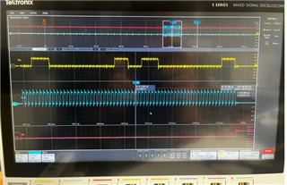
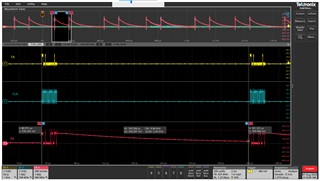
I am requesting SPI master FIFO transfers by enabling the TX interrupt every ~5000 CPU cycles. However, I am seeing that the time from when I enable the TX FIFO interrupt to the interrupt triggering is ~15000 CPU cycles.
Here is how I'm requesting a transfer:
// Processes
// Start sequence of SPI Master read/write register operations to Resolver chip - Blocking
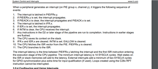
void SpiMaster_StartTransfer(GE_Primary_Container_t *pContainer, uint32_t command)
{
TxEnd = GetProfilerCycles();
TxTime = CalcProfilerTime(TxStart, TxEnd);
pContainer->mpSpiMaster->mDataRecv = 0;
// Reset Rx and Tx Buffers
SPIMaster_ResetBuffers(pContainer);
// TransferData
pContainer->mpSpiMaster->mTxData[0] = (command >> 24) & 0xFFU;
pContainer->mpSpiMaster->mTxData[1] = (command >> 16) & 0xFFU;
pContainer->mpSpiMaster->mTxData[2] = (command >> 8) & 0xFFU;
pContainer->mpSpiMaster->mTxData[3] = (command & 0xFFU);
pContainer->mpSpiMaster->mIsTransferCompleted = false;
// Reset FIFO
SPI_disableFIFO(REPC_RES_DSPI_MASTER_BASEADDR);
SPI_enableFIFO(REPC_RES_DSPI_MASTER_BASEADDR);
SPI_setFIFOInterruptLevel(REPC_RES_DSPI_MASTER_BASEADDR, SPI_FIFO_TXEMPTY, SPI_FIFO_RX4);
// Enable TxFIFO
SPI_enableInterrupt(REPC_RES_DSPI_MASTER_BASEADDR, SPI_INT_TXFF);
SPI_enableInterrupt(REPC_RES_DSPI_MASTER_BASEADDR, SPI_INT_RXFF);
TxStart = GetProfilerCycles();
Tx2Start = GetProfilerCycles();
}
volatile int32_t start = 0;
volatile uint32_t end = 0;
volatile uint32_t RxDelay = 0;
// ISR Routines
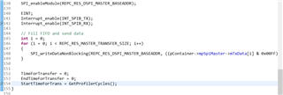
void spiTxFIFOISRRoutine(GE_Primary_Container_t *pContainer)
{
Tx2End = GetProfilerCycles();
Tx2Time = CalcProfilerTime(Tx2Start, Tx2End);
int i = 0;
for (i = 0; i < REPC_RES_MASTER_TRANSFER_SIZE; i++)
{
SPI_writeDataNonBlocking(REPC_RES_DSPI_MASTER_BASEADDR, ((pContainer->mpSpiMaster->mTxData[i] & 0x00FF) << 8));
}
// Do nothing on Tx (we initiate this manually)
SPI_clearInterruptStatus(REPC_RES_DSPI_MASTER_BASEADDR, SPI_INT_TXFF);
Interrupt_clearACKGroup(INTERRUPT_ACK_GROUP6);
// Disable interrupt until next time we're ready to send
SPI_disableInterrupt(REPC_RES_DSPI_MASTER_BASEADDR, SPI_INT_TXFF);
start = GetProfilerCycles();
}
void spiRxFIFOISRRoutine(GE_Primary_Container_t *pContainer)
{
if(!pContainer->mpSpiMaster->mIsTransferCompleted)
{
// We should get 32 bits back
int i = 0;
for (i = 0; i < REPC_RES_MASTER_TRANSFER_SIZE; i++)
{
pContainer->mpSpiMaster->mRxData[i] = (SPI_readDataNonBlocking(REPC_RES_DSPI_MASTER_BASEADDR) & 0x00FF);
}
pContainer->mpSpiMaster->mIsTransferCompleted = true;
end = GetProfilerCycles();
RxDelay = CalcProfilerTime(start, end);
}
SPI_clearInterruptStatus(REPC_RES_DSPI_MASTER_BASEADDR, SPI_INT_RXFF);
Interrupt_clearACKGroup(INTERRUPT_ACK_GROUP6);
// Disable interrupt until next time we're ready to send
SPI_disableInterrupt(REPC_RES_DSPI_MASTER_BASEADDR, SPI_INT_RXFF);
}
Here is my initialization code:
// Init SPI1 Interface to resolver
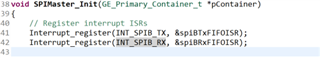
void SPIMaster_Init(GE_Primary_Container_t *pContainer)
{
// Register interrupt ISRs
Interrupt_register(INT_SPIB_TX, &spiBTxFIFOISR);
Interrupt_register(INT_SPIB_RX, &spiBRxFIFOISR);
// Must put SPI into reset before configuring it
SPI_disableModule(REPC_RES_DSPI_MASTER_BASEADDR);
// SPI configuration. Use a 12.5MHz SPICLK and 32-bit word size, 25MHz LSPCLK
// Rising edge SPI
SPI_setConfig(REPC_RES_DSPI_MASTER_BASEADDR, REPC_RES_DSPI_MASTER_CLK_SRC, SPI_PROT_POL0PHA0,
SPI_MODE_MASTER, REPC_RES_TRANSFER_BAUDRATE, 8U);
SPI_disableLoopback(REPC_RES_DSPI_MASTER_BASEADDR);
SPI_setEmulationMode(REPC_RES_DSPI_MASTER_BASEADDR, SPI_EMULATION_FREE_RUN);
SPI_enableFIFO(REPC_RES_DSPI_MASTER_BASEADDR);
SPI_setFIFOInterruptLevel(REPC_RES_DSPI_MASTER_BASEADDR, SPI_FIFO_TXEMPTY, SPI_FIFO_RX4);
SPI_clearInterruptStatus(REPC_RES_DSPI_MASTER_BASEADDR, SPI_INT_TXFF);
SPI_clearInterruptStatus(REPC_RES_DSPI_MASTER_BASEADDR, SPI_INT_RXFF);
SPI_enableInterrupt(REPC_RES_DSPI_MASTER_BASEADDR, SPI_INT_RXFF);
// Configuration complete. Enable the module.
SPI_enableModule(REPC_RES_DSPI_MASTER_BASEADDR);
// Enable interrupts
Interrupt_enable(INT_SPIB_TX);
Interrupt_enable(INT_SPIB_RX);
// Init Master Buffers to 0
SPIMaster_ResetBuffers(pContainer);
// Init Control Variables
pContainer->mpSpiMaster->mIsTransferCompleted = false;
}
I thought maybe it was a priority issue. I'm requesting transfers from Group1 ADCA1_INT with priority 12 so I set my priority for Group 6 SPIB_TX and SPIB_RX to 6.
//###########################################################################
//
// FILE:    sw_prioritized_isr_levels.h
//
// TITLE:   Software Prioritized Interrupt Service Routine Level
//          definitions.
//
//#############################################################################
//
//
// $Copyright:
// Copyright (C) 2021 Texas Instruments Incorporated - http://www.ti.com/
//
// Redistribution and use in source and binary forms, with or without
// modification, are permitted provided that the following conditions
// are met:
//
//   Redistributions of source code must retain the above copyright
//   notice, this list of conditions and the following disclaimer.
//
//   Redistributions in binary form must reproduce the above copyright
//   notice, this list of conditions and the following disclaimer in the
//   documentation and/or other materials provided with the
//   distribution.
//
//   Neither the name of Texas Instruments Incorporated nor the names of
//   its contributors may be used to endorse or promote products derived
//   from this software without specific prior written permission.
//
// THIS SOFTWARE IS PROVIDED BY THE COPYRIGHT HOLDERS AND CONTRIBUTORS
// "AS IS" AND ANY EXPRESS OR IMPLIED WARRANTIES, INCLUDING, BUT NOT
// LIMITED TO, THE IMPLIED WARRANTIES OF MERCHANTABILITY AND FITNESS FOR
// A PARTICULAR PURPOSE ARE DISCLAIMED. IN NO EVENT SHALL THE COPYRIGHT
// OWNER OR CONTRIBUTORS BE LIABLE FOR ANY DIRECT, INDIRECT, INCIDENTAL,
// SPECIAL, EXEMPLARY, OR CONSEQUENTIAL DAMAGES (INCLUDING, BUT NOT
// LIMITED TO, PROCUREMENT OF SUBSTITUTE GOODS OR SERVICES; LOSS OF USE,
// DATA, OR PROFITS; OR BUSINESS INTERRUPTION) HOWEVER CAUSED AND ON ANY
// THEORY OF LIABILITY, WHETHER IN CONTRACT, STRICT LIABILITY, OR TORT
// (INCLUDING NEGLIGENCE OR OTHERWISE) ARISING IN ANY WAY OUT OF THE USE
// OF THIS SOFTWARE, EVEN IF ADVISED OF THE POSSIBILITY OF SUCH DAMAGE.
// $
//#############################################################################
#ifndef SW_PRIORITZIED_ISR_LEVELS_H
#define SW_PRIORITZIED_ISR_LEVELS_H

#ifdef __cplusplus
extern "C" {
#endif

//
// Mask for interrupt groups
//
#define M_INT1      0x0001  // INT1 Mask
#define M_INT2      0x0002  // INT2 Mask
#define M_INT3      0x0004  // INT3 Mask
#define M_INT4      0x0008  // INT4 Mask
#define M_INT5      0x0010  // INT5 Mask
#define M_INT6      0x0020  // INT6 Mask
#define M_INT7      0x0040  // INT7 Mask
#define M_INT8      0x0080  // INT8 Mask
#define M_INT9      0x0100  // INT9 Mask
#define M_INT10     0x0200  // INT10 Mask
#define M_INT11     0x0400  // INT11 Mask
#define M_INT12     0x0800  // INT12 Mask
#define M_INT13     0x1000  // INT13 Mask
#define M_INT14     0x2000  // INT14 Mask
#define M_DLOG      0x4000  // DLOGINT Mask
#define M_RTOS      0x8000  // RTOSINT Mask

//
// Interrupt Enable Register Allocation:
// Interrupts can be enabled/disabled using the CPU interrupt enable register
// (IER) and the PIE interrupt enable registers (PIEIER1 to PIEIER12).
//

//
// Set "Global" Interrupt Priority Level (IER register):
//
// The user must set the appropriate priority level for each of the CPU
// interrupts. This is termed as the "global" priority. The priority level
// must be a number between 1 (highest) to 16 (lowest). A value of 0 must
// be entered for reserved interrupts or interrupts that are not used.
//
// Note: The priority levels below are used to calculate the IER register
//       interrupt masks MINT1 to MINT16.
//
// Note: The priority levels shown here may not make sense in a
//       real application.  This is for demonstration purposes only!!!
//
//       The user should change these to values that make sense for
//       their application.
//
// 0  = not used
// 1  = highest priority
// ...
// 16 = lowest priority
//
#define INT1PL      12       // Global Priority for Group1 Interrupts
#define INT2PL      0        // Global Priority for Group2 Interrupts
#define INT3PL      0        // Global Priority for Group3 Interrupts
#define INT4PL      0        // Global Priority for Group4 Interrupts
#define INT5PL      0        // Global Priority for Group5 Interrupts
#define INT6PL      6        // Global Priority for Group6 Interrupts
#define INT7PL      15        // Global Priority for Group7 Interrupts
#define INT8PL      0        // Global Priority for Group8 Interrupts
#define INT9PL      15        // Global Priority for Group9 Interrupts
#define INT10PL     0        // Global Priority for Group10 Interrupts
#define INT11PL     0        // Global Priority for Group11 Interrupts
#define INT12PL     14        // Global Priority for Group12 Interrupts
#define INT13PL     0        // Global Priority for INT13 (TINT1)
#define INT14PL     0        // Global Priority for INT14 (TINT2)
#define INT15PL     0        // Global Priority for DATALOG
#define INT16PL     0        // Global Priority for RTOSINT

//
// Set "Group" Interrupt Priority Level (PIEIER1 to PIEIER12 registers):
//
// The user must set the appropriate priority level for each of the PIE
// interrupts. This is termed as the "group" priority. The priority level
// must be a number between 1 (highest) to 16 (lowest). A value of 0 must
// be entered for reserved interrupts or interrupts that are not used.
//
// Note: The priority levels below are used to calculate the following
//       PIEIER register interrupt masks:
//       MG1_1 to MG1_16
//       MG2_1 to MG2_16
//       MG3_1 to MG3_16
//       MG4_1 to MG4_16
//       MG5_1 to MG5_16
//       MG6_1 to MG6_16
//       MG7_1 to MG7_16
//       MG8_1 to MG8_16
//       MG9_1 to MG9_16
//       MG10_1 to MG10_16
//       MG11_1 to MG11_16
//       MG12_1 to MG12_16
//
// Note: The priority levels shown here may not make sense in a
//       real application.  This is for demonstration purposes only!!!
//
//       The user should change these to values that make sense for
//       their application.
//
// 0  = not used
// 1  = highest priority
// ...
// 16  = lowest priority
//
#define G1_1PL      12       // ADCA1_INT
#define G1_2PL      12       // ADCB1_INT
#define G1_3PL      12       // ADCC1_INT
#define G1_4PL      14       // XINT1_INT
#define G1_5PL      14       // XINT2_INT
#define G1_6PL      0       // Reserved
#define G1_7PL      14       // TIMER0_INT
#define G1_8PL      0       // WAKE_INT
#define G1_9PL      0       // Reserved
#define G1_10PL     0       // Reserved
#define G1_11PL     0       // Reserved
#define G1_12PL     0       // Reserved
#define G1_13PL     0       // Reserved
#define G1_14PL     0       // Reserved
#define G1_15PL     0       // Reserved
#define G1_16PL     0       // Reserved

#define G2_1PL      0       // EPWM1_TZ_INT
#define G2_2PL      0       // EPWM2_TZ_INT
#define G2_3PL      0       // EPWM3_TZ_INT
#define G2_4PL      0       // EPWM4_TZ_INT
#define G2_5PL      0       // EPWM5_TZ_INT
#define G2_6PL      0       // EPWM6_TZ_INT
#define G2_7PL      0       // EPWM7_TZ_INT
#define G2_8PL      0       // EPWM8_TZ_INT
#define G2_9PL      0       // Reserved
#define G2_10PL     0       // Reserved
#define G2_11PL     0       // Reserved
#define G2_12PL     0       // Reserved
#define G2_13PL     0       // Reserved
#define G2_14PL     0       // Reserved
#define G2_15PL     0       // Reserved
#define G2_16PL     0       // Reserved

#define G3_1PL      0       // EPWM1_INT
#define G3_2PL      0       // EPWM2_INT
#define G3_3PL      0       // EPWM3_INT
#define G3_4PL      0       // EPWM4_INT
#define G3_5PL      0       // EPWM5_INT
#define G3_6PL      0       // EPWM6_INT
#define G3_7PL      0       // EPWM7_INT
#define G3_8PL      0       // EPWM8_INT
#define G3_9PL      0       // Reserved
#define G3_10PL     0       // Reserved
#define G3_11PL     0       // Reserved
#define G3_12PL     0       // Reserved
#define G3_13PL     0       // Reserved
#define G3_14PL     0       // Reserved
#define G3_15PL     0       // Reserved
#define G3_16PL     0       // Reserved

#define G4_1PL      0       // ECAP1_INT
#define G4_2PL      0       // ECAP2_INT
#define G4_3PL      0       // ECAP3_INT
#define G4_4PL      0       // ECAP4_INT
#define G4_5PL      0       // ECAP5_INT
#define G4_6PL      0       // ECAP6_INT
#define G4_7PL      0       // ECAP7_INT
#define G4_8PL      0       // Reserved
#define G4_9PL      0       // Reserved
#define G4_10PL     0       // Reserved
#define G4_11PL     0       // Reserved
#define G4_12PL     0       // Reserved
#define G4_13PL     0       // Reserved
#define G4_14PL     0       // ECAP6_2_INT
#define G4_15PL     0       // ECAP7_2_INT
#define G4_16PL     0       // Reserved

#define G5_1PL      0       // EQEP1_INT
#define G5_2PL      0       // EQEP2_INT
#define G5_3PL      0       // Reserved
#define G5_4PL      0       // Reserved
#define G5_5PL      0       // CLB1_INT
#define G5_6PL      0       // CLB2_INT
#define G5_7PL      0       // CLB3_INT
#define G5_8PL      0       // CLB4_INT
#define G5_9PL      0       // SD1_INT
#define G5_10PL     0       // Reserved
#define G5_11PL     0       // Reserved
#define G5_12PL     0       // Reserved
#define G5_13PL     0       // SDFM1DR1_INT
#define G5_14PL     0       // SDFM1DR2_INT
#define G5_15PL     0       // SDFM1DR3_INT
#define G5_16PL     0       // SDFM1DR4_INT

#define G6_1PL      6       // SPIA_RX_INT
#define G6_2PL      6       // SPIA_TX_INT
#define G6_3PL      6       // SPIB_RX_INT
#define G6_4PL      6       // SPIB_TX_INT
#define G6_5PL      0       // Reserved
#define G6_6PL      0       // Reserved
#define G6_7PL      0       // Reserved
#define G6_8PL      0       // Reserved
#define G6_9PL      0       // Reserved
#define G6_10PL     0       // Reserved
#define G6_11PL     0       // Reserved
#define G6_12PL     0       // Reserved
#define G6_13PL     0       // Reserved
#define G6_14PL     0       // Reserved
#define G6_15PL     0       // Reserved
#define G6_16PL     0       // Reserved

#define G7_1PL      0       // DMA_CH1_INT
#define G7_2PL      0       // DMA_CH2_INT
#define G7_3PL      0       // DMA_CH3_INT
#define G7_4PL      0       // DMA_CH4_INT
#define G7_5PL      13       // DMA_CH5_INT
#define G7_6PL      13       // DMA_CH6_INT
#define G7_7PL      0       // Reserved
#define G7_8PL      0       // Reserved
#define G7_9PL      0       // Reserved
#define G7_10PL     0       // Reserved
#define G7_11PL     0       // FSITXA1_INT
#define G7_12PL     0       // FSITXA2_INT
#define G7_13PL     0       // FSIRXA1_INT
#define G7_14PL     0       // FSIRXA2_INT
#define G7_15PL     0       // CLA1PROMCRC_INT
#define G7_16PL     0       // DCC_INT

#define G8_1PL      0       // I2CA_INT
#define G8_2PL      0       // I2CA_FIFO_INT
#define G8_3PL      0       // Reserved
#define G8_4PL      0       // Reserved
#define G8_5PL      0       // Reserved
#define G8_6PL      0       // Reserved
#define G8_7PL      0       // Reserved
#define G8_8PL      0       // Reserved
#define G8_9PL      0       // LINA0_INT
#define G8_10PL     0       // LINA1_INT
#define G8_11PL     0       // Reserved
#define G8_12PL     0       // Reserved
#define G8_13PL     0       // PMBUSA_INT
#define G8_14PL     0       // Reserved
#define G8_15PL     0       // Reserved
#define G8_16PL     0       // Reserved

#define G9_1PL      13       // SCIA_RX_INT
#define G9_2PL      13       // SCIA_TX_INT
#define G9_3PL      0       // SCIB_RX_INT
#define G9_4PL      0       // SCIB_TX_INT
#define G9_5PL      0       // CANA0_INT
#define G9_6PL      0       // CANA1_INT
#define G9_7PL      0       // CANB0_INT
#define G9_8PL      0       // CANB1_INT
#define G9_9PL      0       // Reserved
#define G9_10PL     0       // Reserved
#define G9_11PL     0       // Reserved
#define G9_12PL     0       // Reserved
#define G9_13PL     0       // Reserved
#define G9_14PL     0       // Reserved
#define G9_15PL     0       // Reserved
#define G9_16PL     0       // Reserved

#define G10_1PL     0       // ADCA_EVT_INT
#define G10_2PL     0       // ADCA2_INT
#define G10_3PL     0       // ADCA3_INT
#define G10_4PL     0       // ADCA4_INT
#define G10_5PL     0       // ADCB_EVT_INT
#define G10_6PL     0       // ADCB2_INT
#define G10_7PL     0       // ADCB3_INT
#define G10_8PL     0       // ADCB4_INT
#define G10_9PL     0       // ADCC_EVT_INT
#define G10_10PL    0       // ADCC2_INT
#define G10_11PL    0       // ADCC3_INT
#define G10_12PL    0       // ADCC4_INT
#define G10_13PL    0       // Reserved
#define G10_14PL    0       // Reserved
#define G10_15PL    0       // Reserved
#define G10_16PL    0       // Reserved

#define G11_1PL     0       // CLA1_1_INT
#define G11_2PL     0       // CLA1_2_INT
#define G11_3PL     0       // CLA1_3_INT
#define G11_4PL     0       // CLA1_4_INT
#define G11_5PL     0       // CLA1_5_INT
#define G11_6PL     0       // CLA1_6_INT
#define G11_7PL     0       // CLA1_7_INT
#define G11_8PL     0       // CLA1_8_INT
#define G11_9PL     0       // Reserved
#define G11_10PL    0       // Reserved
#define G11_11PL    0       // Reserved
#define G11_12PL    0       // Reserved
#define G11_13PL    0       // Reserved
#define G11_14PL    0       // Reserved
#define G11_15PL    0       // Reserved
#define G11_16PL    0       // Reserved

#define G12_1PL     14       // XINT3_INT
#define G12_2PL     0       // XINT4_INT
#define G12_3PL     0       // XINT5_INT
#define G12_4PL     0       // PBIST_INT
#define G12_5PL     0       // FMC_INT
#define G12_6PL     0       // VCU_INT
#define G12_7PL     0       // FPU_OVERFLOW_ISR
#define G12_8PL     0       // FPU_UNDERFLOW_ISR
#define G12_9PL     0       // Reserved
#define G12_10PL    0       // RAM_CORRECTABLE_ERROR_ISR
#define G12_11PL    0       // FLASH_CORRECTABLE_ERROR_ISR
#define G12_12PL    0       // RAM_ACCESS_VIOLATION_INT
#define G12_13PL    0       // SYS_PLL_SLIP_INT
#define G12_14PL    0       // Reserved
#define G12_15PL    0       // CLA_OVERFLOW_INT
#define G12_16PL    0       // CLA_UNDERFLOW_INT

//
// Include the header file with software interrupt prioritization logic
//
#include "sw_interrupt_prioritization_logic.h"

#ifdef __cplusplus
}
#endif /* extern "C" */

#endif // eof

//
// End of file
//
Do you have any ideas what I'm doing to cause the TX FIFO interrupt to take so long to trigger?