Other Parts Discussed in Thread: TIDM-02000, C2000WARE
Hello. I am trying to recreate the software control described in TIDM-02000 for a Full Bridge Converter. I'm using 4 PWMs for switching. EPWM1A/B and EPWM2A/B are complimentary PWMs. I want EPWM1A/B to react to the comparator when a sensed voltage reaches a ramped reference. I try to use EPWM3 to reset the ramp reference at the beginning of every EPWM2A/B period.
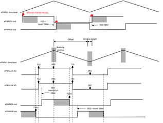
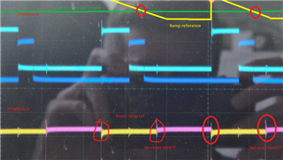
To test if the comparator turns off the EPWM1A/B correctly I use a power supply to the comparator input to see if the duty cycle of EPWM1A/B is affected. Here I get unexpected behaviour. I think something is wrong with the way I reset the ramp reference but I am not sure.
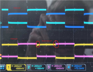
Here is without any voltage to the comparator. Behaving as expected
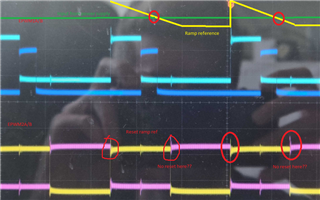
Here I apply some voltage to the comparator. I expect the EPWM1A/B to behave the same, but they dont. I drew what I think is going on with the ramp reference but I am not sure. Can you see what I am doing wrong?
//###########################################################################
//
// FILE:   Example_2806xEPwmDeadBand.c
//

//
// Included Files
//
#include "DSP28x_Project.h"     // Device Headerfile and Examples Include File

//
// Function Prototypes
//
void InitEPwm1Example(void);
void InitEPwm2Example(void);
void InitEPwm3Example(void);
__interrupt void epwm1_isr(void);
__interrupt void epwm2_isr(void);
__interrupt void epwm3_isr(void);

//
// Globals
//
Uint32  EPwm1TimerIntCount;
Uint32  EPwm2TimerIntCount;
Uint32  EPwm3TimerIntCount;
Uint16  EPwm1_DB_Direction;
Uint16  EPwm2_DB_Direction;
Uint16  EPwm3_DB_Direction;

//
// Defines that Maximum Dead Band values
//
#define EPWM1_MAX_DB   0x0000
#define EPWM2_MAX_DB   0x0000
#define EPWM3_MAX_DB   0x0000

#define EPWM1_MIN_DB   0
#define EPWM2_MIN_DB   0
#define EPWM3_MIN_DB   0

//
// Defines to keep track of which way the Dead Band is moving
//
#define DB_UP   1
#define DB_DOWN 0

//
// Main
//
void main(void)
{
    //
    // Step 1. Initialize System Control:
    // PLL, WatchDog, enable Peripheral Clocks
    // This example function is found in the F2806x_SysCtrl.c file.
    //
    InitSysCtrl();

    //
    // Step 2. Initalize GPIO:
    // This example function is found in the F2806x_Gpio.c file and
    // illustrates how to set the GPIO to it's default state.
    //
    // InitGpio();  // Skipped for this example

    //
    // For this case just init GPIO pins for ePWM1, ePWM2, ePWM3
    // These functions are in the F2806x_EPwm.c file

    EALLOW;
       SysCtrlRegs.PCLKCR0.bit.ADCENCLK = 1;     // Enable Clock to the ADC

       //
       // Comparator shares the internal BG reference of the ADC, must be powered
       // even if ADC is unused
       //
       AdcRegs.ADCCTL1.bit.ADCBGPWD = 1;

       DELAY_US(1000);							  // Delay for Power Up

       //
       // Enable clock to the Comparator 1 block
       //
       SysCtrlRegs.PCLKCR3.bit.COMP1ENCLK = 1;

       Comp1Regs.COMPCTL.bit.COMPDACEN = 1;      // Power up Comparator 1 locally
       //Comp1Regs.DACCTL.bit.DACSOURCE = 0;

       Comp1Regs.DACCTL.bit.DACSOURCE = 1;  // Ramp
       Comp1Regs.DACCTL.bit.RAMPSOURCE = 0x2;  // PWM3 sync
       EPwm3Regs.HRPCTL.bit.PWMSYNCSEL = 1; // PWMSYNC is generated by TBCTR = 0 pulse. Reset Ramp reference
       Comp1Regs.RAMPMAXREF_SHDW = 0xFFFF;
       Comp1Regs.RAMPDECVAL_SHDW = 0x5F;


       // Connect the inverting input to the internal DAC
       //
       Comp1Regs.COMPCTL.bit.COMPSOURCE = 0;
       //Comp1Regs.DACVAL.bit.DACVAL = 512;	    // Set DAC output to midpoint
       //
       SysCtrlRegs.PCLKCR0.bit.TBCLKSYNC = 0;
       EDIS;


    //
    InitEPwm1Gpio();
    InitEPwm2Gpio();
    InitEPwm3Gpio();

    EALLOW;
    SysCtrlRegs.PCLKCR0.bit.TBCLKSYNC = 1;
    EDIS;

    //
    // Step 3. Clear all interrupts and initialize PIE vector table:
    // Disable CPU interrupts
    //
    DINT;

    //
    // Initialize the PIE control registers to their default state.
    // The default state is all PIE interrupts disabled and flags
    // are cleared.
    // This function is found in the F2806x_PieCtrl.c file.
    //
    InitPieCtrl();

    //
    // Disable CPU interrupts and clear all CPU interrupt flags
    //
    IER = 0x0000;
    IFR = 0x0000;

    //
    // Initialize the PIE vector table with pointers to the shell Interrupt
    // Service Routines (ISR).
    // This will populate the entire table, even if the interrupt
    // is not used in this example.  This is useful for debug purposes.
    // The shell ISR routines are found in F2806x_DefaultIsr.c.
    // This function is found in F2806x_PieVect.c.
    //
    InitPieVectTable();

    //
    // Interrupts that are used in this example are re-mapped to
    // ISR functions found within this file.
    //
    EALLOW;  // This is needed to write to EALLOW protected registers
    PieVectTable.EPWM1_INT = &epwm1_isr;
    PieVectTable.EPWM2_INT = &epwm2_isr;
    PieVectTable.EPWM3_INT = &epwm3_isr;
    EDIS;    // This is needed to disable write to EALLOW protected registers

    //
    // Step 4. Initialize all the Device Peripherals:
    // This function is found in F2806x_InitPeripherals.c
    //
    // InitPeripherals();  // Not required for this example

    EALLOW;
    SysCtrlRegs.PCLKCR0.bit.TBCLKSYNC = 0;
    EDIS;

    InitEPwm1Example();
    InitEPwm2Example();
    InitEPwm3Example();

    EALLOW;
    SysCtrlRegs.PCLKCR0.bit.TBCLKSYNC = 1;
    EDIS;

    //
    // Step 5. User specific code, enable interrupts
    // Initalize counters:
    //
    EPwm1TimerIntCount = 0;
    EPwm2TimerIntCount = 0;
    EPwm3TimerIntCount = 0;

    //
    // Enable CPU INT3 which is connected to EPWM1-3 INT
    //
    IER |= M_INT3;

    //
    // Enable EPWM INTn in the PIE: Group 3 interrupt 1-3
    //
    PieCtrlRegs.PIEIER3.bit.INTx1 = 1;
    PieCtrlRegs.PIEIER3.bit.INTx2 = 1;
    PieCtrlRegs.PIEIER3.bit.INTx3 = 1;

    //
    // Enable global Interrupts and higher priority real-time debug events
    //
    EINT;   // Enable Global interrupt INTM
    ERTM;   // Enable Global realtime interrupt DBGM

    //
    // Step 6. IDLE loop. Just sit and loop forever (optional)
    //
    for(;;)
    {
        __asm("          NOP");
    }
}

//
// epwm1_isr -
//
__interrupt void
epwm1_isr(void)
{
    EPwm1TimerIntCount++;

    //
    // Clear INT flag for this timer
    //
    EPwm1Regs.ETCLR.bit.INT = 1;

    //
    // Acknowledge this interrupt to receive more interrupts from group 3
    //
    PieCtrlRegs.PIEACK.all = PIEACK_GROUP3;
}

//
// epwm2_isr -
//
__interrupt void
epwm2_isr(void)
{

    EPwm2TimerIntCount++;

    //
    // Clear INT flag for this timer
    //
    EPwm2Regs.ETCLR.bit.INT = 1;

    //
    // Acknowledge this interrupt to receive more interrupts from group 3
    //
    PieCtrlRegs.PIEACK.all = PIEACK_GROUP3;
}

//
// epwm3_isr -
//
__interrupt void
epwm3_isr(void)
{


    EPwm3TimerIntCount++;

    //
    // Clear INT flag for this timer
    //
    EPwm3Regs.ETCLR.bit.INT = 1;

    //
    // Acknowledge this interrupt to receive more interrupts from group 3
    //
    PieCtrlRegs.PIEACK.all = PIEACK_GROUP3;
}

//
// InitEPwm1Example -
//
void
InitEPwm1Example()
{

	EALLOW;
    EPwm1Regs.TBPRD = 300;                        // Set timer period
    EPwm1Regs.TBPHS.half.TBPHS = 0x0000;           // Phase is 0
    EPwm1Regs.TBCTR = 0x0000;                      // Clear counter

    //
    // Setup TBCLK
    //
    EPwm1Regs.TBCTL.bit.CTRMODE = TB_COUNT_UPDOWN; // Count up
    EPwm1Regs.TBCTL.bit.PHSEN = TB_DISABLE;        // Disable phase loading
    EPwm1Regs.TBCTL.bit.HSPCLKDIV = 1;       // Clock ratio to SYSCLKOUT
    EPwm1Regs.TBCTL.bit.CLKDIV = 0;
    EPwm1Regs.TBCTL.bit.SYNCOSEL = 2;       // = CMPB

    EPwm1Regs.CMPCTL.bit.SHDWAMODE = CC_SHADOW;    // Load registers every ZERO
    EPwm1Regs.CMPCTL.bit.SHDWBMODE = CC_SHADOW;
    EPwm1Regs.CMPCTL.bit.LOADAMODE = CC_CTR_ZERO;
    EPwm1Regs.CMPCTL.bit.LOADBMODE = CC_CTR_ZERO;


    //
    // Setup compare
    //
    EPwm1Regs.CMPA.half.CMPA = 150;
    EPwm1Regs.CMPB = 150;

    //
    // Set actions
    //
    EPwm1Regs.AQCTLA.bit.CBU = AQ_SET;              // Set PWM3A on CAU
    EPwm1Regs.AQCTLA.bit.CBD = AQ_CLEAR;            // Clear PWM3A on CAD

    EPwm1Regs.AQCTLB.bit.CBU = AQ_CLEAR;            // Clear PWM3B on CAU
    EPwm1Regs.AQCTLB.bit.CBD = AQ_SET;              // Set PWM3B on CAD


    //

    //
    EPwm1Regs.DBCTL.bit.OUT_MODE = DB_FULL_ENABLE; // 0x3
    EPwm1Regs.DBCTL.bit.POLSEL = DB_ACTV_HIC;      // 0x2
    EPwm1Regs.DBCTL.bit.IN_MODE = DBA_ALL;         // 0x0
    EPwm1Regs.DBRED = EPWM2_MAX_DB;
    EPwm1Regs.DBFED = EPWM2_MAX_DB;
    EPwm1_DB_Direction = DB_UP;

    //

    //
    EPwm1Regs.ETSEL.bit.INTSEL = ET_CTR_ZERO;     // Select INT on Zero event
    //EPwm2Regs.ETSEL.bit.INTEN = 1;                // Enable INT
    EPwm1Regs.ETPS.bit.INTPRD = ET_3RD;           // Generate INT on 3rd event


    //--- Setup for forcing EPWM1A/B low when input voltage reaches ramp reference


    EPwm1Regs.DCTRIPSEL.bit.DCAHCOMPSEL = DC_COMP1OUT; // DCAH = Comparator 1 output
    EPwm1Regs.DCTRIPSEL.bit.DCBHCOMPSEL = DC_COMP1OUT;

    EPwm1Regs.TZDCSEL.bit.DCAEVT2 = TZ_DCAH_HI; // DCAEVT2 = DCAH high(will become active
    EPwm1Regs.TZDCSEL.bit.DCBEVT2 = TZ_DCBH_HI;

    EPwm1Regs.DCACTL.bit.EVT2SRCSEL = DC_EVT2; // DCAEVT2 = DCAEVT2 (not filtered)
    EPwm1Regs.DCACTL.bit.EVT2FRCSYNCSEL = DC_EVT_ASYNC; // Take async path // Enable DCAEVT2 as a

    EPwm1Regs.DCBCTL.bit.EVT2SRCSEL = DC_EVT2; // DCAEVT2 = DCAEVT2 (not filtered)
    EPwm1Regs.DCBCTL.bit.EVT2FRCSYNCSEL = DC_EVT_ASYNC; // Take async path // Enable DCAEVT2 as a
    // one-shot trip source
    // Note: DCxEVT1 events can be defined as
    // one-shot.
    // DCxEVT2 events can be defined as
    // cycle-by-cycle.
    EPwm1Regs.TZSEL.bit.DCAEVT2 = 1;
    EPwm1Regs.TZSEL.bit.DCBEVT2 = 1; // What do we want the DCAEVT1 and DCBEVT1
    // events to do?

    // DCAEVTx events can force EPWMxA
    // DCBEVTx events can force EPWMxB
    EPwm1Regs.TZCTL.bit.TZA = TZ_FORCE_LO; // EPWM1A will go low
    EPwm1Regs.TZCTL.bit.TZB = TZ_FORCE_LO; // EPWM1B will go low
EDIS;

}

//
// InitEPwm2Example -
//
void
InitEPwm2Example()
{
    EPwm2Regs.TBPRD = 300;                         // Set timer period
    EPwm2Regs.TBPHS.half.TBPHS = 0x0000;            // Phase is 0
    EPwm2Regs.TBCTR = 0x0000;                       // Clear counter

    //
    // Setup TBCLK
    //
    EPwm2Regs.TBCTL.bit.CTRMODE = TB_COUNT_UPDOWN; // Count up
    EPwm2Regs.TBCTL.bit.PHSEN = TB_DISABLE;        // Disable phase loading
    EPwm2Regs.TBCTL.bit.HSPCLKDIV = 1;       // Clock ratio to SYSCLKOUT
    EPwm2Regs.TBCTL.bit.SYNCOSEL = 1;   // Time-base counter equal to zero (TBCTR = 0x0000). In order to sync EPWM3

    //
    // Slow so we can observe on the scope
    //
    EPwm2Regs.TBCTL.bit.CLKDIV = 0;

    //
    // Setup compare
    //
    EPwm2Regs.CMPA.half.CMPA = 150;

    //
    // Set actions
    //
    EPwm2Regs.AQCTLA.bit.ZRO = AQ_SET;           // Set PWM1A on CAU
    EPwm2Regs.AQCTLA.bit.PRD = AQ_CLEAR;		 // Clear PWM1A on CAD

    EPwm2Regs.AQCTLB.bit.ZRO = AQ_CLEAR;         // Clear PWM1B on CAU
    EPwm2Regs.AQCTLB.bit.PRD = AQ_SET;           // Set PWM1B on CAD

    //
    // Active high complementary PWMs - Setup the deadband
    //
    EPwm2Regs.DBCTL.bit.OUT_MODE = DB_FULL_ENABLE; // 0x3
    EPwm2Regs.DBCTL.bit.POLSEL = DB_ACTV_HIC;      // 0x2
    EPwm2Regs.DBCTL.bit.IN_MODE = DBA_ALL;         // 0x0
    EPwm2Regs.DBRED = EPWM2_MAX_DB;
    EPwm2Regs.DBFED = EPWM2_MAX_DB;
    EPwm2_DB_Direction = DB_UP;

    //
    //
    //
    EPwm2Regs.ETSEL.bit.INTSEL = ET_CTR_ZERO;     // Select INT on Zero event
    //EPwm2Regs.ETSEL.bit.INTEN = 1;                // Enable INT
    EPwm2Regs.ETPS.bit.INTPRD = ET_3RD;           // Generate INT on 3rd event
}

//
// InitEPwm3Example -
//
void
InitEPwm3Example()
{
    EPwm3Regs.TBPRD = 300;                         // Set timer period
    EPwm3Regs.TBPHS.half.TBPHS = 0;            // Phase is 0
    EPwm3Regs.TBCTR = 0;                       // Clear counter

    //
    // Setup TBCLK
    //
    EPwm3Regs.TBCTL.bit.CTRMODE = TB_COUNT_DOWN; // Count down
    EPwm3Regs.TBCTL.bit.PHSEN = 1;        // Enable phase loading
    EPwm3Regs.TBCTL.bit.HSPCLKDIV = 1;       // Clock ratio to SYSCLKOUT


    //
    EPwm3Regs.TBCTL.bit.CLKDIV = 0;

    //
    // Setup compare
    //
    EPwm3Regs.CMPB = 150;

    //
    // Set actions
    //
    EPwm3Regs.AQCTLA.bit.ZRO = AQ_SET;              // Set PWM3A on CAU
    EPwm3Regs.AQCTLA.bit.CBD = AQ_CLEAR;            // Clear PWM3A on CAD

    EPwm3Regs.AQCTLB.bit.ZRO = AQ_CLEAR;            // Clear PWM3B on CAU
    EPwm3Regs.AQCTLB.bit.CBD = AQ_SET;              // Set PWM3B on CAD

    //

    //
    //
    //
    EPwm3Regs.ETSEL.bit.INTSEL = ET_CTR_ZERO;     // Select INT on Zero event
    //EPwm2Regs.ETSEL.bit.INTEN = 1;                // Enable INT
    EPwm3Regs.ETPS.bit.INTPRD = ET_3RD;           // Generate INT on 3rd event
}

//
// End of File
//