This thread has been locked.

If you have a related question, please click the "Ask a related question" button in the top right corner. The newly created question will be automatically linked to this question.

C2000WARE: Programming with jtag XDS100V2 error on TMS320F28377DGWTEP

Part Number: C2000WARE
Other Parts Discussed in Thread: TMDSCNCD28379D, SN74LVC3G07

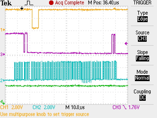
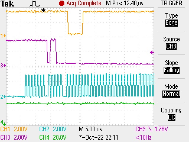
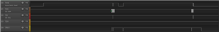
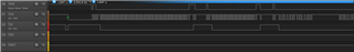
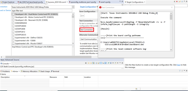
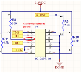
Hello, i have a TMDSCNCD28379D with a dev kit, is their anyway to manually test JTAG connection with xds100v2 black hawk that i purchased? We designed a board with a TMS320F28377DGWTEP but are having issues with our jtag programming. Attached is how we ha 
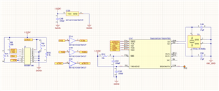
ve our JTAG connected to our processor if anyone can help.

  • Is there a pinout sheet that should tell me what the voltage is on each pin, or what the outputs should be so i can read them?

  • Hi Jonathan,

    I would be curious to see what happens when you use CCS to launch the Target Configuration for the CCS Project, then use the 'Test Connection' option. This tests the JTAG connection to your device, and its output log may give some clues about what is going wrong. Please post your output log from 'Test Connection'. 

    If you are able to look at your signals with an oscilloscope, you should see the same patterns as I do when I 'Test Connection' to my device with the XDS100V2. The image below shows TDO (yellow), TMS (purple), TCK (blue), and TRST (green). This is the start of the 'Test Connection' sequence that I captured as a single sequence, triggered on the falling edge of TMS. All signals are 3.3V digital signals.

    If you zoom in more closely, you should see this same pattern at the start. 

    Please let me know if you see something different, or if you notice signal integrity issues when you look at you signals on the oscilloscope.

    If you would like to know more about what the signals are doing, I would recommend that you read about the JTAG TAP state machine, and the IR and DR registers, though that may not be necessary to debug this. 

    Best Regards,

    Ben Collier

  • Hello, this is what i receive. Oddly enough, i don't see TDO resetting.

  • Here are some voltage reading from a oscilloscope. 
    Channel 1: TMS
    Channel 2: CLK
    Channel 3: TDI
    Channel 4: RST


  • Hi Jonathan,

    Thank you for providing the images. Would it be possible to zoom into the start of the oscilloscope capture, so that we could see the individual clock pulses? Again, please trigger the single capture on the falling edge of TMS and do a 'Test Connection'. Also, could you post the output log from 'Test Connection'? You could just copy and paste it into the reply if you like. 

    Best Regards,

    Ben Collier

  • [Start: Texas Instruments XDS110 USB Debug Probe_0]Execute the command:%ccs_base%/common/uscif/dbgjtag -f %boarddatafile% -rv -o -S integrity[Result]-----[Print the board config pathname(s)]------------------------------------C:\Users\Eric\AppData\Local\Texas Instruments\
        CCS\ccs1040\0\0\BrdDat\testBoard.dat-----[Print the reset-command software log-file]-----------------------------This utility has selected a 100- or 510-class product.
    This utility will load the adapter 'jioxds110.dll'.
    The library build date was 'Jun 25 2021'.
    The library build time was '11:45:30'.
    The library package version is '9.4.0.00129'.
    The library component version is '35.35.0.0'.
    The controller does not use a programmable FPGA.
    The controller has a version number of '5' (0x00000005).
    The controller has an insertion length of '0' (0x00000000).
    This utility will attempt to reset the controller.
    This utility has successfully reset the controller.-----[Print the reset-command hardware log-file]-----------------------------The scan-path will be reset by toggling the JTAG TRST signal.
    The controller is the XDS110 with USB interface.
    The link from controller to target is direct (without cable).
    The software is configured for XDS110 features.
    The controller cannot monitor the value on the EMU[0] pin.
    The controller cannot monitor the value on the EMU[1] pin.
    The controller cannot control the timing on output pins.
    The controller cannot control the timing on input pins.
    The scan-path link-delay has been set to exactly '0' (0x0000).-----[An error has occurred and this utility has aborted]--------------------This error is generated by TI's USCIF driver or utilities.The value is '-233' (0xffffff17).
    The title is 'SC_ERR_PATH_BROKEN'.The explanation is:
    The JTAG IR and DR scan-paths cannot circulate bits, they may be broken.
    An attempt to scan the JTAG scan-path has failed.
    The target's JTAG scan-path appears to be broken
    with a stuck-at-ones or stuck-at-zero fault.[End: Texas Instruments XDS110 USB Debug Probe_0]

    Heres the test connection results. I forgot to mention that we connected pin 5, to ground by accident in our schematic but we fixed the board but we might have fried the XDS110V2 debug prob. I attached a image and highlighted in red where the 3v3 is shorted to ground. Do you think that can fry the debugger? I'll try and get some better oscilloscope pictures. 

  • Heres some more images on our digital analyzer

  • Hi Jonathan,

    I do not think that would fry your debugger. Could you also try testing connection with the XDS100-V2 and posting that log? I am trying to determine if there is a problem with the physical scan path, and it is not yet clear to me from this log, as this error could be caused by a few things. You may also want to try 'Test Connection' with a lower TCK frequency and see if that changes the output. The setting for the TCK frequency can be found in the 'Advanced' Tab of the Target Configuration. 

    Also, if you provide further Oscilloscope or Logic Analyzer images, please let me know how the captures were obtained, and zoom until the individual clock pulses are visible. For example, you could trigger the scope to take a single capture at the rising/falling edge of the 'Test Connection'/'Connect Target' sequence with the XDS100V2/XDS110 and changing any of those options would result in a different pattern. I am trying to compare the patterns you send me with known good patterns to see if there are any obvious differences, so I need to know the full context. 

    Best Regards,

    Ben Collier

  • Hello, My colleague found some information that may help us find the issue. 

    When reading the output of a our TMS,NTRST,AND TDI from the output of the buffer we have, we do not see any output on NTRST. 
    On the developer board, we noticed that the resistor that is connected to ground on the NTRST line was AFTER the buffer. ours is before it. We are unsure if that is the issue if you can provide anything on that. 

    I attached a photo of our TDI,TMS, AND NTRST lines.

    our buffer is a SN74LVC3G07DCUT.

    the processor we are using : TMS320F28377DGWTEP

    debugger: xds110NTRST ISSUE.docx

  • i also attached more information based on his words from what he did. Extra ntrst issue details.docx

  • Hi Jonathan,

    I am a little unclear on the current state of your setup. Is the resistor now wired at the buffer output, or still at the input? If you test connection, what TRST signal are you seeing at the input to the MCU? I'm also not sure if TRST needs to be buffered at all, is it possible to hardwire the TRST signal from the debugger directly to the MCU? Also, were all of the oscilloscope and logic analyzer signals that you previously posted taken physically at the debugger port? 

    Best Regards,

    Ben Collier 

  • Hello, this is from my colleague:


    All of the screenshots were taken off of the debugger tool, not the input of the MCU. The BGA makes it difficult taking direct measurements off the MCU lines, however we were able to probe the output of the buffer that connects to the MCU and verify the CLK and TMS signals are passing through the same signals seen at the debugger port.

    At the moment, the 2.2k resistor to ground on the input to the buffer has been moved to the output of the buffer, pulling the MCU line down. The resulting signal read on the line going directly to the MCU is able to detect a logic signal that only achieves .7V but does appear to be a scaled down version of the previously measured signal coming off the debugger tool.

  • Hi Jonathan,

    So the TRST signal going to the MCU is only .7V? While the CLK and TMS signals going to the MCU are 3.3V? That will certainly cause issues. If you remove the resistor entirely, will you get 3.3V at the buffer output? Or is it possible to hardwire the TRST signal from the JTAG header directly to the MCU trace somehow? Somehow, we need to get the TRST signal close to 3.3V and to the MCU. If this causes signal integrity issues, we can try lowering the TCK frequency. 

    When you test connection, make sure to lower the TCK frequency to something like 1 MHz following the guidelines I mentioned in a previous response. If the TRST path is unreliable, Test Connection may fail at the default 5.5MHz, but pass at some lower frequency.  

    Best Regards,

    Ben Collier

  • From my colleague:


    We have tested at lower frequencies without any luck. When the pull down resistor is removed, the voltage appears as a random wave pattern that doesn't go higher than 50mV. Right now, the trace to the input of the buffer was cut to help isolate it but the trace on the output is still connected as I am tappinging a connection to the pad of the buffer. I would need to cut that trace as well to fully isolate the MCU connection to the debugger and retest.

  • Hi Jonathan,

    Yeah, my suggestion is to try lower frequencies once the TRST signal is able to reach close to 3.3V at the MCU. For now it should fail regardless.

    I would be curious to see if your setup would work with the TRST wired from the debugger directly to the MCU, but I understand that is not easy to test, and that is not the most robust solution. 

    Unfortunately I am not very knowledgeable about the SN74LVC3G07, and I am not sure why you cannot get 3.3V at the buffer output for the TRST signal. If you would like support to debug that specific issue, I would recommend making a separate E2E post in the logic forum. 

    Of course I would be happy to continue supporting with the JTAG issue to the best of my abilities.

    Best Regards,

    Ben Collier

  • We seem to have something work without the buffer, but another error we gotta dive into. Good way to end a Friday so I'll get back if everything goes well next week.

  • Hi Jonathan,

    That sounds like some good news, I will be waiting for an update next week.

    Best Regards,
    Ben Collier

  • Happy news, kinda .

    We found the buffer was the issue. due to it being a open drain on the output for nTRST , the single stayed high and that caused the issue. Now we can program the board which is nice. 

    Hopefully everything else goes well and just a small board design will need to be done. 

    thanks!

  • Ok, that's good to hear! Please let me know if you have any further issues with programming your device. 

    Best Regards,

    Ben Collier