This thread has been locked.

If you have a related question, please click the "Ask a related question" button in the top right corner. The newly created question will be automatically linked to this question.

TMS320F280049C: Understanding hystresis feature of CMPSS

Part Number: TMS320F280049C

Hi,

I'm planning to use hysteresis feature of CMPSS. I saw a register named as COMPHYSCTL. I'm connected ADCINB6 to positive input of high comparator and DAC ref to negative input of high comparator. And now, I need to set hysteresis and determine two threshold levels. Please, help on it.

The explanation of COMPHYSCTL is like below.

"

Comparator hysteresis. Sets the amount of hysteresis on the
comparator inputs.
0 None
1 Set to typical hysteresis
2 Set to 2x of typical hysteresis
3 Set to 3x of typical hysteresis
4 Set to 4x of typical hysteresis

"

There is also another information as below.

But I cannot understand above and conflict about the information. what "4x of typical hysteresis" is? of what hysteresis?

1) What does it mean "4x of typical hysteresis" ? What is typical hysteresis? Which value is multiplied by 4? Please, provide formula in order to get me understand fully.

2) By writing 4 to COMPHYSCTL is enough to set hysteresis?

3) What is the meaning of explanation in (1) at above table? It say that CMPSS DAC is used as reference. However, I set COMPHYSCTL to control hysteresis? What is the relationship between COMPHYSCTL  and CMPS DAC reference? How both of them scale the hysteresis? Which drives really the hystresis?

4) I inserted below the real analog comparator with hysteresis. There is connectionn between positive input and output of comparator. It provides hystresis. However, I couldn't set relationship for inside of MCU. I only connect ADC inputs to CMPSS inputs.
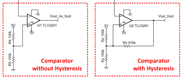
5) How can I determine High threshold and low threshold?

Thank you in advance.

  • Hello,

    Thank you for your patience.

    1) Generally, hysteresis helps the comparator avoid oscillation due to small amounts of variations. A comparator with hysteresis presents one trip point for the rising input voltage (VH) and one for the falling input voltage (VL). The difference between these trip points is the hysteresis band, shown in Figure 7-50.

    If the voltage of COMPINxP goes higher than CMPINxN (or DACxVAL), the output goes HIGH. On the other hand, if the voltage of COMPINxP goes less than total voltage of CMPINxN plus Hysteresis, the output goes LOW.


    From Comparator Electrical Characteristics, the typical hysteresis is 12 LSB. The LSB can be calculated using the following formula:


    For instance, for this device N=12 and if we use VDDA=3.3V, then the LSB is equal to 805 uV.

    If the Hysteresis is 4X, the hysteresis is equal to 4×12×805 uV = 38.64 mV.

    2) Yes, you just need to write 4 to COMPHYSCT.

     3) The explanation (1) means that the Hysteresis depends on the DAC reference voltage. As I mentioned above, the formula for LSB calculation implies that the LSB changes based on the FSR value. If we select the DAC reference voltage, FSR is equal to DAC reference voltage. So, the LSB value will be different than the LSB value when we select voltage VDDA.

     4) In the comparator with hysteresis, there is two threshold voltages: VL and VH. In Figure 7-50, if the voltage of COMPINxP goes higher than CMPINxN (or DACxVAL), the output goes HIGH. On the other hand, if the voltage of COMPINxP goes less than total voltage of CMPINxN plus Hysteresis, the output goes LOW. In fact, in MCU, the value of Rth is adjusted in a way that we can have different values of threshold voltages VL and VH.

    Regards,

    Hadi

  • Dear Hadi,

    Your explanation is really helpful. Thank you for it. I need one more step.

    1) What does FSR mean? Is it full scale range? Please, explain.

    2) Is " N=12 " written in any document? Please, refer. How could I find out?

    3) What is the value of N  for the TMS320F280048?

    3) Is VDDA used in calculations DAC reference? If I change DAC reference from VDDA to VDAC, does it mitigate to VDAC in calculations?

    4) LSB is least significant bit. What does "N= 12" mean LSB=12?

    5) Is the "typical hysteresis" written in any document? Does 1x mean typical? 

    6) So, if I use 4x hysteresis and VDAC out = 1.65V, the VH=1.65V and  VL=1.65-38.64mV.

    7) How much can I increase hysetresis as a maximum?

    8) Please, correct me. As a conclusion, the hysteresis depends on the connection made to negative input of comparator. Hysteresis depends on FSR and FSR changes depending on the selection of inverting input of comparator. If internal DAC is used FSR=VDAC, and if other external input is connected FSR=VDDA of MCU? If I change hysteresis, the formula will be HYSTERESIS SELECTED * 12 * 805 uV for TMS320F280049C.?

    9) Could you please correct below figure?

    Thank you in advance.

  • Dear Gokhan,

    You're welcome.

    1) Yes, it stands for full scale range, which is the range defined by the reference inputs of the ADC.

    2) It is mentioned in the datasheet of device that there is 12-bit reference Digital-to-Analog Converters (DACs), https://www.ti.com/lit/gpn/tms320f280049c

    3) Based on the datasheet, N is equal to 12.

    4) In the table given in datasheet, the CMPSS DAC is used as the reference for hysteresis. In the example I gave in the previous response I used VDDA= 3.3 V. If you use the DAC value, then your FSR would be equal to DAC value.

    5) As you know, LSB is least significant bit, which can be calculated using formula

    6) The typical value of hysteresis is 1x or 12LSB, which has been mentioned in Table 16-5 in Technical reference manual, TMS320F28004x Real-Time Microcontrollers Technical Reference Manual (Rev. E).

    7) Yes, that’s correct.

    8) The maximum value is 4x, which in this case is equal to 38.64 mV.

    9) The hysteresis doesn’t depend on the voltage of the inverting pin. In fact, as mentioned in Table given in section 7.10.5.1.1, Comparator Electrical Characteristics, in datasheet, the hysteresis depends on DAC reference voltage. Based on table given in section 7.10.4.1.1 Buffered DAC Operating Conditions in datasheet, the DAC reference value can be 2.4V ~VDDA.

    10) The value of FSR is not defined correctly. In fact, FSR changes based on the reference voltage, which can be VDDA or DAC reference voltage.

    Regards,

    Hadi