This thread has been locked.

If you have a related question, please click the "Ask a related question" button in the top right corner. The newly created question will be automatically linked to this question.

F28M35H52C: Unable to Program C28 side - Error 1015

Part Number: F28M35H52C
Other Parts Discussed in Thread: UNIFLASH, SN74HC03, SN74HC00

Contract Manufacturer here that has made a new revision of a PCB and now I am unable to program the C28 side of the CPU through the FTDI (FT2232HL) USB programmer. I can however program the M3 side without an issue AND my customer has been able to program the C28 side using a Spectrum JTAG programmer. I receive this error while trying to load flash into the C28:

Texas Instruments XDS100v2 USB Debug Probe/C28xx_0

Error connecting to the target: (Error -1015 @ 0x0) Device is not responding to the request. Device may be locked, or the debug probe connection may be unreliable. Unlock the device if possible (e.g. use wait in reset mode, and power-cycle the board). If error persists, confirm configuration and/or try more reliable JTAG settings (e.g. lower TCLK). (Emulation package 9.9.0.00040)

I have 5 boards. They all exhibit the same behavior while trying to program the C28 via the XDS100v2. I did not change the JTAG circuit at all in the PCB revision (unless there is a manufacturing issue with the boards) and this problem did not persist on the the previous boards. 3 of the new boards are using CPUs that were removed from the previous revisions board and 2 have brand new CPUs. The 3 that were removed from previous boards already were programed and the code runs but I am unable to erase or reprogram them now (C28 side).

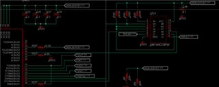
The XDS100v2 debugger is powered by the USB port and isolated from the CPU. On these new boards I did have to change the isolators from a ISO7241 to a ISO7231 b/c I could not get the ISO7241. Both are 25Mbps so I don't see why that would be the issue. I have done 'test connection' tests in Code Composer and with JP1 & JP2 on, succeed at all TCLK speeds.

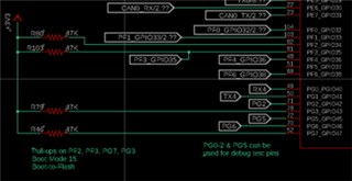
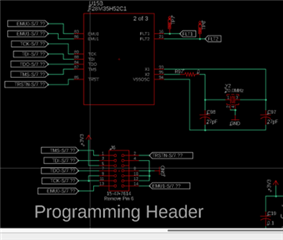
Below are the relevant parts of the schematic. The CPU is on the +3V3-GND side and the FTDI chip is on the DEBUG3V3-GND1 side. JP1 jumper is installed to program via USB and removed to program from the 14 pin JTAG header. I am not sure what the purpose of the JP2 jumper is. It is required to make one of the JTAG tests succeed but is not required to program the M3 side. CPU is set to boot in MODE 15 - Boot from Flash

My procedure for programming the boards has been to gradually increase voltage on the new board making sure all the voltage regulators work. I then plug in the USB cord, test voltages, open FTDI Prog, apply and program the XDS100 template to the FTDI chip. I then install the JP1 & JP2 jumper, open Code Composer and do a 'Connection Test' on the JTAG. I then open UniFlash and program the M3. I then try to program the C28 and get the above error. I have tried using slower TCLK down to 10kHz. I have erased the M3 and tried to program the C28 first. I have changed R41 and R67 to 2.2K (EMU pull ups) and have removed R20 (TCLK pull up).

It appears as if the JTAG connection is good from the successful connection test and being able to program the M3. I don't believe the C28 side of the CPU is bad because using a JTAG programmer it can be programmed and is running the code. What can I check or do from here?

Thanks for your help.

 -


  • Hi, 

    Your query has been forwarded to an expert, pls expect a response by tomorrow.

    Best Regards

    Siddharth

  • Hi Eric,

    Thank you for your question. I'll need some more time to look over the hardware schematics, but I'll get back to you tomorrow. 

    Thanks,

    Charles

  • Thank you, I look forward to your assistance with this. Let me know if you need anything else.

  • Hi Eric,

    Some software/hardware questions I have for you:

    1) When connecting the XDS100v2 debugger and connecting to CCS, are you manually trying to connect the target configuration (.ccxml) file for the device, to see if it is in the locked state (without clicking the debug button)? I assume you are using the JP1 & JP2 wires to do this.

    2) Have you made sure that the TRSTn pin is not in a floating state? It could be affecting the CPU.  The schematic is a bit blurry, what side is this pin on?

    3) Would programming the C28 side first make a difference?

    Thanks,

    Charles

  • Charles

    1) Sorry I'm not very experienced with CCS. I would assume I am connecting manually. I am not connecting via debug. While in CCS I have a tab with the *.ccxml file name open and I can click through the tabs to change the TCLK and some other settings. This is the location I do the 'Test Connection' test. I then save this file and open it in UniFlash. UniFlash is what I use to program the chip. JP1 & JP2 are connected during this processes.

    2) I have a 2.2K pull down (R24) on the TRSTn pin. This is between the output of the digital isolator and the TI chip. I also have a pulldown resistor (R21) between the FTDI chip and the digital isolator that has normally been DNP. I have tried a pull down on it as well without success.

    3) I have erased the M3 side and attempted to program the C28 first. That too was unsuccessful.

  • Hi Eric,

    I see that the C28x flashing sequence did not even start since you are having trouble connecting to it.  Hence, this is not a flash programming issue.

    Assuming that C28x is not locked by security:

    1) When trying to connect to the C28x, what is the state of the M3?  Is it in halt state?  Or is it executing?  If executing, try halting it.

    2) Try programming the C28x after keeping the device boot pins in boot from serial peripheral mode and see if that helps.

    3) Is device powered via USB port of the laptop?  If yes, can you instead try powering the board from an external supply?

    4) Do you see any toggle on the XRSn pin when C28x fails to connect?

    Thanks and regards,

    Vamsi

  • Vamsi, thank you for your assistance

    1) I have tried with the M3 executing and while erased. Same result

    2) Same error when booting in Boot Mode 2 (PG7 tied high)

    3) The CPU is powered (+3V3) by an external power supply. The Debug3V3 is powered by the laptop. It just powers the FTDI chip and the digital isolators. I have put a scope on it and haven't noticed any power dips while trying to program.

    4) With the M3 erased and the ARS & XSR separated and floating I appear to be getting a WDR pulse on the XRS. It is @ 25uSec every 1mSec. I see random pulses on the ARS. They are 25uSec as well but happen in an inconsistent manner. With the M3 executing I will see some pulses of the XRS but I believe it is the code preforming a reset since the C28 is not running. I also get an LED flash at the same time that is an indication of a software reset. I do not see any XRS activity corresponding to an attempt to connect.

    Regards, Eric

  • Hi Eric,

    1) and 4): I mean to try when M3 is halted - not when executing an erased flash (causes ITRAP) or application. 

    I will assign this to a board expert to see if they have any further suggestion.  

    Thanks and regards,
    Vamsi

  • Vamsi, I am not familiar with how to do that. What is the procedure to Halt the M3? I will give it a try. I've only had to just program these. I haven't been involved with any development or debug.

  • Eric,

    Would it be possible to ZIP the images at full resolution and attach them to the post vs inline?  I can't zoom in effectively and having trouble reading everything.

    Just to clarify, did the previous HW with the 4 channel isolator chip/XDS100 work OK?  I think the answer is yes, but wanted to make sure I understand that. 

    To Vamsi's last point he was asking to connect to the device/M3 core  via Code Composer (via the XDS100 connection), halt the M3 and then see if the XDS100 can connect to the C28x core.

    This video should explain how to do that(it is using CCSv5, but that shouldn't matter), in case you have only been using UniFlash to interact with the device. https://training.ti.com/concerto-f28m3x-microcontroller-training-part-9-code-composer-studio-emulation

    Best,

    Matthew

  • Here is a pdf of the schematic parts. Hopefully this is better.

    The previous chip did work without issue.

    Thank you for the instruction on connecting to the core. I will try it shortly and report the results.

    TI Schematic.pdf

  • I was able to start the debug session and connect to the M3. I suspended it (assume the same as HALT). This would pause the operation of the chip as the blinking LEDs would stop. I could load a program to it. All seems good.

    I tried to connect to the C28 and get the same -1015 error with or without the M3 suspended.

  • Eric,

    Can you probe EMU0/EMU1 at the local C2000 pin and note the value when you are trying to connect, or even just when the board is powered with no JTAG connected?

    If these are treated the same even with different isolators I'm not sure why there would be a difference, but I know that standard ARM does not use these pins and C28x does(sampled on the rising edge of TRSTn).  Maybe more a hunch/clue why ARM is OK and C28x is not.

    We want to see both as high/VDDIO level when trying to connect(for normal operation). 

    Best,

    Matthew

  • Matthew, THANK YOU! for this incite. Looking at this I found both the EMU0 & EMU1 where low on the C2000 side. They had no voltage change no matter what I tried. If I removed the JP1 (enable USB programming) jumper then EMU1 would go high telling me that the digital isolator (U9) was holding it low. I then started to look into that circuit. I am not sure what exactly the U14 SN74HC03 does but I found it is a NAND gate with open collector outputs. Probing the lines I found that one of the outputs should have been high but without any pull up resistors it was still low. I added pull up resistors to EMU0 & EMU1 on pins 3 & 4 of U9 and now I can connect and program the C28 side. Not sure why this worked on previous boards. I will have to look into that but for now this has solved this problem. Your help was greatly appreciated.

  • Found that the previously used ISO7241 digital isolators had internal 1Meg pull up resistors on the inputs. The ISO7341 used on this build (could not find any ISO7241 instock) do not have internal pull ups on the inputs therefore the outputs 2Y (EMU0) and 3Y (EMU1) of the SN74HC03 were never able to go to a logic 1. Going to replace the SN74HC03 with a SN74HC00 so the output are push pull instead of open drain.

  • Eric,

    Glad we could help, I saw the NAND chip, but I didn't catch that it was OC config with no pulls. 

    Let us know if you have anymore questions.

    Best,

    Matthew