This thread has been locked.

If you have a related question, please click the "Ask a related question" button in the top right corner. The newly created question will be automatically linked to this question.

TMS320F28377D: Flash Memory Writing Error & Recognition chip Error

Part Number: TMS320F28377D
Other Parts Discussed in Thread: C2000WARE

Dear, Sir.

My Development Environment is that i use TMS320F28377DZWTS, (System Clock : 20MHz) and SDS200i (JTAG Clcok : 10MHz) emulator.

https://www.tms320f28x.co.kr/goods/goods_view.php?goodsNo=200903075#support

The distance between JTAG connector and DSP is within 80mm.


Q1)

The following error occurred in flash memory writing less 20 times.

 What could be causing this error ?

 What are the measures to prevent recurrence ?


Q2)

The following error occurred in flash memory writing less 20 times.

DSP cannot be recognized by CCS.

Watch Dog Reset seems to keep happening.

It is known to occur when flash memory writing is incompletely terminated.

RAM mode doesn’t work. Wait Mode boot doesn’t work


 What could be causing this error ?

 What are the measures to prevent recurrence ?


  • Hi Kim,

    I don't think your problem is being caused by JTAG connectivity issues, but could you post the output log from Testing Connection to your device just to confirm? So when you use Code Composer Studio to open the Target Configuration for the CCS Project, use the 'Test Connection' option. If the test succeeds, then something other than the JTAG connection is the source of the problem.

    I will also reach out to one of our other experts to assist you further with this issue.

    Best Regards,

    Ben Collier

  • Kim,

              When you say “20 times”, are you saying you were able to program the device fine 20 times and now you are seeing this problem?

  • Dear Benjamin Collier,

    Upload the requested data as follows.

    [Development Environment]

    Emulator : BH560V2 (JTAG CLK : 10Mhz)

    CCS Ver : v11.2.0

    C2000ware Ver : V4.1.1

    1. The same experiment was performed by changing the emulator (from SDS200i to BH560V2),

        but the result was the same.

       Flash memory download full log record attached. (LOOO_30_Flash_DW_Log.txt)

    2. There is no error in JTAG Clock scan result with BH560V2. (BH560v2_connection_test_log.txt)

    3. It seeems that  a specific area of flash memory is damaged.

        What could be the cause of  such damage ?

    Best Regards,

    Jaehyung Kim,

    C28xx_CPU1: GEL Output: 
    Memory Map Initialization Complete
    C28xx_CPU1: If erase/program (E/P) operation is being done on one core, the other core should not execute from shared-RAM (SR) as they are used for the E/P code. Also, CPU1 will be halted to determine SR ownership for the CPU which will run the Flash Plugin code, after which CPU1 will be set to run its application. User code execution from SR could commence after both flash banks are programmed.
    C28xx_CPU1: Error during Flash programming (Flash algorithm returned error code). FMSTAT (STATCMD on some devices) value = 4112. Operation Cancelled (0).
    C28xx_CPU1: File Loader: Memory write failed: Unknown error
    C28xx_CPU1: GEL: File: C:\CCS\4.1.CCS (2)\LSAM_TestFirmware_20220405\LOOM_TestCode_6STEP_V1_8_cpu1.out: Load failed.
    C28xx_CPU1: Writing Flash @ Address 0x00080000 of Length 0x00000002 (page 0)
    C28xx_CPU1: PLL configuration status = 1. PLL configured successfully.
    C28xx_CPU1: Erasing Flash Bank 0, Sector A
    C28xx_CPU1: Erasing Flash Bank 0, Sector B
    C28xx_CPU1: Erasing Flash Bank 0, Sector C
    C28xx_CPU1: Erasing Flash Bank 0, Sector D
    C28xx_CPU1: Erasing Flash Bank 0, Sector E
    C28xx_CPU1: Erasing Flash Bank 0, Sector F
    C28xx_CPU1: Erasing Flash Bank 0, Sector G
    C28xx_CPU1: Erasing Flash Bank 0, Sector H
    C28xx_CPU1: Erasing Flash Bank 0, Sector I
    C28xx_CPU1: Erasing Flash Bank 0, Sector J
    C28xx_CPU1: Erasing Flash Bank 0, Sector K
    C28xx_CPU1: Erasing Flash Bank 0, Sector L
    C28xx_CPU1: Erasing Flash Bank 0, Sector M
    C28xx_CPU1: Erasing Flash Bank 0, Sector N
    C28xx_CPU1: Data has been buffered at the end of the current data block for 64-bit aligned writes.
    C28xx_CPU1: Writing Flash @ Address 0x00082000 of Length 0x00000190 (page 0)
    C28xx_CPU1: Verifying Flash @ Address 0x00082000 of Length 0x00000320
    C28xx_CPU1: Writing Flash @ Address 0x00082190 of Length 0x00001e70 (page 0)
    C28xx_CPU1: Verifying Flash @ Address 0x00082190 of Length 0x00003CE0
    C28xx_CPU1: Writing Flash @ Address 0x00084000 of Length 0x00000d6f (page 0)
    C28xx_CPU1: Data has been buffered at the end of the current data block for 64-bit aligned writes.
    C28xx_CPU1: Verifying Flash @ Address 0x00084000 of Length 0x00001AD8
    C28xx_CPU1: Writing Flash @ Address 0x00086000 of Length 0x00000135 (page 0)
    C28xx_CPU1: Data has been buffered at the end of the current data block for 64-bit aligned writes.
    C28xx_CPU1: Verifying Flash @ Address 0x00086000 of Length 0x00000268
    C28xx_CPU1: Writing Flash @ Address 0x00090000 of Length 0x0000061e (page 0)
    C28xx_CPU1: Data has been buffered at the end of the current data block for 64-bit aligned writes.
    C28xx_CPU1: Error during Flash programming (Flash algorithm returned error code). FMSTAT (STATCMD on some devices) value = 4112. Operation Cancelled (0).
    C28xx_CPU1: File Loader: Memory write failed: Unknown error
    C28xx_CPU1: GEL: File: C:\CCS\4.1.CCS (2)\LSAM_TestFirmware_20220405\LOOM_TestCode_6STEP_V1_8_cpu1.out: Load failed.
    C28xx_CPU1: Writing buffered data @ Address 0x00080000 of Length 0x00000004
    C28xx_CPU1: Verifying Flash @ Address 0x00080000 of Length 0x00000008
    C28xx_CPU1: Writing buffered data @ Address 0x00084D6C of Length 0x00000004
    C28xx_CPU1: Verifying Flash @ Address 0x00084D6C of Length 0x00000008
    C28xx_CPU1: Writing buffered data @ Address 0x00086134 of Length 0x00000004
    C28xx_CPU1: Verifying Flash @ Address 0x00086134 of Length 0x00000008
    C28xx_CPU1: Writing buffered data @ Address 0x0009061C of Length 0x00000004
    C28xx_CPU1: Verifying Flash @ Address 0x0009061C of Length 0x00000008

    [Start: Blackhawk XDS560v2-USB System Trace Emulator_0]
    
    Execute the command:
    
    %ccs_base%/common/uscif/dbgjtag.exe -f %boarddatafile% -rv -o -F inform,logfile=yes -S pathlength -S integrity
    
    [Result]
    
    
    -----[Print the board config pathname(s)]------------------------------------
    
    C:\Users\garam\AppData\Local\TEXASI~1\CCS\
        ccs1120\0\0\BrdDat\testBoard.dat
    
    -----[Print the reset-command software log-file]-----------------------------
    
    This utility has selected a 560/2xx-class product.
    This utility will load the program 'bh560v2u.out'.
    Loaded FPGA Image: C:\ti\ccs1120\ccs\ccs_base\common\uscif\dtc_top.jbc
    The library build date was 'Mar 17 2022'.
    The library build time was '19:00:32'.
    The library package version is '9.7.0.00213'.
    The library component version is '35.35.0.0'.
    The controller does not use a programmable FPGA.
    The controller has a version number of '6' (0x00000006).
    The controller has an insertion length of '0' (0x00000000).
    The cable+pod has a version number of '8' (0x00000008).
    The cable+pod has a capability number of '7423' (0x00001cff).
    This utility will attempt to reset the controller.
    This utility has successfully reset the controller.
    
    -----[Print the reset-command hardware log-file]-----------------------------
    
    The scan-path will be reset by toggling the JTAG TRST signal.
    The controller is the Nano-TBC VHDL.
    The link is a 560-class second-generation-560 cable.
    The software is configured for Nano-TBC VHDL features.
    The controller will be software reset via its registers.
    The controller has a logic ONE on its EMU[0] input pin.
    The controller has a logic ONE on its EMU[1] input pin.
    The controller will use falling-edge timing on output pins.
    The controller cannot control the timing on input pins.
    The scan-path link-delay has been set to exactly '2' (0x0002).
    The utility logic has not previously detected a power-loss.
    The utility logic is not currently detecting a power-loss.
    Loaded FPGA Image: C:\ti\ccs1120\ccs\ccs_base\common\uscif\dtc_top.jbc
    
    -----[The log-file for the JTAG TCLK output generated from the PLL]----------
    
      Test  Size   Coord      MHz    Flag  Result       Description
      ~~~~  ~~~~  ~~~~~~~  ~~~~~~~~  ~~~~  ~~~~~~~~~~~  ~~~~~~~~~~~~~~~~~~~
        1   none  - 01 00  500.0kHz   -    similar      isit internal clock
        2   none  - 01 09  570.3kHz   -    similar      isit internal clock
        3     64  - 01 00  500.0kHz   O    good value   measure path length
        4     16  - 01 00  500.0kHz   O    good value   auto step initial
        5     16  - 01 0D  601.6kHz   O    good value   auto step delta
        6     16  - 01 1C  718.8kHz   O    good value   auto step delta
        7     16  - 01 2E  859.4kHz   O    good value   auto step delta
        8     16  + 00 02  1.031MHz   O    good value   auto step delta
        9     16  + 00 0F  1.234MHz   O    good value   auto step delta
       10     16  + 00 1F  1.484MHz   O    good value   auto step delta
       11     16  + 00 32  1.781MHz   O    good value   auto step delta
       12     16  + 01 04  2.125MHz   O    good value   auto step delta
       13     16  + 01 11  2.531MHz   O    good value   auto step delta
       14     16  + 01 21  3.031MHz   O    good value   auto step delta
       15     16  + 01 34  3.625MHz   O    good value   auto step delta
       16     16  + 02 05  4.313MHz   O    good value   auto step delta
       17     16  + 02 13  5.188MHz   O    good value   auto step delta
       18     16  + 02 23  6.188MHz   O    good value   auto step delta
       19     16  + 02 37  7.438MHz   O    good value   auto step delta
       20     16  + 03 07  8.875MHz   O    good value   auto step delta
       21     16  + 03 15  10.63MHz   O    good value   auto step delta
       22     16  + 03 1E  11.75MHz  {O}   good value   auto step delta
       23     64  + 02 3E  7.875MHz   O    good value   auto power initial
       24     64  + 03 0E  9.750MHz   O    good value   auto power delta
       25     64  + 03 16  10.75MHz   O    good value   auto power delta
       26     64  + 03 1A  11.25MHz   O    good value   auto power delta
       27     64  + 03 1C  11.50MHz   O    good value   auto power delta
       28     64  + 03 1D  11.63MHz   O    good value   auto power delta
       29     64  + 03 1D  11.63MHz   O    good value   auto power delta
       30     64  + 03 13  10.38MHz  {O}   good value   auto margin initial
    
    The first internal/external clock test resuts are:
    The expect frequency was 500000Hz.
    The actual frequency was 499872Hz.
    The delta frequency was 128Hz.
    
    The second internal/external clock test resuts are:
    The expect frequency was 570312Hz.
    The actual frequency was 569214Hz.
    The delta frequency was 1098Hz.
    
    In the scan-path tests:
    The test length was 2048 bits.
    The JTAG IR length was 6 bits.
    The JTAG DR length was 1 bits.
    
    The IR/DR scan-path tests used 30 frequencies.
    The IR/DR scan-path tests used 500.0kHz as the initial frequency.
    The IR/DR scan-path tests used 11.75MHz as the highest frequency.
    The IR/DR scan-path tests used 10.38MHz as the final frequency.
    
    -----[Measure the source and frequency of the final JTAG TCLKR input]--------
    
    The frequency of the JTAG TCLKR input is measured as 10.37MHz.
    
    The frequency of the JTAG TCLKR input and TCLKO output signals are similar.
    The target system likely uses the TCLKO output from the emulator PLL.
    
    -----[Perform the standard path-length test on the JTAG IR and DR]-----------
    
    This path-length test uses blocks of 64 32-bit words.
    
    The test for the JTAG IR instruction path-length succeeded.
    The JTAG IR instruction path-length is 6 bits.
    
    The test for the JTAG DR bypass path-length succeeded.
    The JTAG DR bypass path-length is 1 bits.
    
    -----[Perform the Integrity scan-test on the JTAG IR]------------------------
    
    This test will use blocks of 64 32-bit words.
    This test will be applied just once.
    
    Do a test using 0xFFFFFFFF.
    Scan tests: 1, skipped: 0, failed: 0
    Do a test using 0x00000000.
    Scan tests: 2, skipped: 0, failed: 0
    Do a test using 0xFE03E0E2.
    Scan tests: 3, skipped: 0, failed: 0
    Do a test using 0x01FC1F1D.
    Scan tests: 4, skipped: 0, failed: 0
    Do a test using 0x5533CCAA.
    Scan tests: 5, skipped: 0, failed: 0
    Do a test using 0xAACC3355.
    Scan tests: 6, skipped: 0, failed: 0
    All of the values were scanned correctly.
    
    The JTAG IR Integrity scan-test has succeeded.
    
    -----[Perform the Integrity scan-test on the JTAG DR]------------------------
    
    This test will use blocks of 64 32-bit words.
    This test will be applied just once.
    
    Do a test using 0xFFFFFFFF.
    Scan tests: 1, skipped: 0, failed: 0
    Do a test using 0x00000000.
    Scan tests: 2, skipped: 0, failed: 0
    Do a test using 0xFE03E0E2.
    Scan tests: 3, skipped: 0, failed: 0
    Do a test using 0x01FC1F1D.
    Scan tests: 4, skipped: 0, failed: 0
    Do a test using 0x5533CCAA.
    Scan tests: 5, skipped: 0, failed: 0
    Do a test using 0xAACC3355.
    Scan tests: 6, skipped: 0, failed: 0
    All of the values were scanned correctly.
    
    The JTAG DR Integrity scan-test has succeeded.
    
    [End: Blackhawk XDS560v2-USB System Trace Emulator_0]
    

  • Dear, Hareesh Janakiraman,

    Worked as below.

    1. The flash memory error occurred in the 15th flash memory download. (Board Number #30)

         - Until the 14th flash download, the DSP operated normally.

         - It works normally in RAM download mode.

         - When download  option setting by turning on the Range Avoidance Settings in CCS and setting range from 0x90000 to 0x91000,

           the download succeeds.


    2.  The DSP recognition error occurred in the 12th flash memory download. (Board Number #37)

        - Until the 11th flash download, the DSP operated normally.

        - But from the 12th flash download, It not works normally in RAM & FLASH download mode.

    Is the SDS200i (syncworks) emulator officially recognized by TI ?

    What are the causes of the above two types of errors ?

    Since it is a problem between DSP and JTAG, i think TI should explain the cause.

    Because i can't check inside the DSP.

    If i send a failed DSP to TI, how long on average will it take to receive the failure analysis results ?

    Best Regards,

    Jaehyung Kim,

  • Hi Jaehyung Kim,

    This is assigned to me today. 

    Please note:  I am out of office.  I will be back to office late next week.  I will review this post and get back to you next week.  Thank you.

    Thanks and regards,

    Vamsi

  • Hi Jaehyung Kim,

    1) Did anything change in the out file between passing and failing flash-load iterations?  If yes, what is it?

    2) Can you take a look at the advisory Low-Power Modes: Power Down Flash or Maintain Minimum Device Activity in the errata and see if that is applicable here since you are running at a lower SYSCLK?

    3) When you look at the memory window where the flash programming failed for you, what contents do you see?  

    Thanks and regards,
    Vamsi

  • Dear Vamsi Gudivada,

    A1) As for upgrading the developed system operating code version 3 to version 4, 
    only 2 boards out of a total of 47 boards had flash memory specific area errors.
    The remaining 45 boards work normally.Flash memory is generally known to allow 100,000 writes.
    There is no action of repeatedly writing a specific area within the code

    A2) We will conduct another experiment within this week and share the results.
    Can I do LPM (Low-Power Modes) when CCS does not even recognize DSP ?

    A3) In the above answer, the entire flash memory write log record is posted in the TXT file.
    Note please.(LOOO_30_Flash_DW_Log.txt)

    Regards,
    Jaehyung Kim,
  • Hi Jaehyung Kim,

    Will get back to you within the next day and look into the LPM/memory log.

    Thanks and regards,

    Charles

  • Dear, Charles Roberson, Vamsi Gudivada,

    Q1 is question about board number 30 (flash memory specific area destruction), and

    Q2 is question about board number 37 (DSP not recognized).

    I tried LPM for board number 37, but it failed because CCS could not recognize the DSP.

    My quess is that when the CCS tries to recognize the DSP, the DSP should abort the watchdog reset, but it doesn't seem to abort.

    P.S) Are the symptoms of Q1 and Q2 a phenomenon that occurs when the DSP is physically damaged ?

    Thanks and regards,

    Charles Roberson, Vamsi Gudivada,

  • Hi Jaehyung Kim,

    Sorry for the delay on our side. Many people are taking time off around the holidays here.

    A3) In the above answer, the entire flash memory write log record is posted in the TXT file.
    Note please.(LOOO_30_Flash_DW_Log.txt)

    The log shows that The memory address range 0x90000 to 0x91000 can't be written to, but Vamsi was asking if you can read from this memory section. After connecting to the device in CCS you can use the Memory Browser tool and enter specific memory addresses to read the data stored. Can you please check the values being read in the 0x90000 to 0x91000 range and provide a screenshot of the Memory Browser?

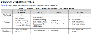
    This SDS200i debug probe isn't a common one we support, listed below. It's possible it could have caused some issue during flash program / erase.

    Best,

    Kevin

  • Dear Kevin Allen18,

    As you requested, i read the memory data near 0x90000 and upload the screenshot and log data.

    Please review.

    LOOO_30_Memory_221226.dat

    Best,

    Jaehyung Kim

  • Kim,

    Kevin is out of office until Thursday January 5th. Please expect response by Friday. Sincere apology for delay in response.

    Regards, Santosh

  • Hi Jaehyung Kim,

    In your linker command file, can you check if there is any address that is not a valid flash address?

    Thanks and regards,
    Vamsi

  • Dear Vamsi Gudivada,

    My linker command file is uploaded.

    Please, review it.

    Thanks and regards.

    Jaehyung Kim,

    2837x_FLASH_lnk_cpu1.zip

  • Hi Kim,

    I will be able to review and get back to you on this Wednesday.

    Thanks and regards,
    Vamsi

  • Hi Kim,

    Linker command file looks ok.  Is this taken from the latest C2000Ware or from an older version?

    Did you make sure that the voltage rails are in the Datasheet spec range when the Flash operations are in progress?

    Thanks and regards,

    Vamsi

  • Dear Vamsi Gudivada,

    1. Supply Voltage (1.2V and 3.3V) waveform is good during flash write.


    2. C2000Ware ver is  4.01.00.00.

    Thanks and regards,

    Jaehyung Kim   

  • Hi Kim,

    How about erase?

    Can you try disabling the watchdog?  Flash API does not enable/disable the watchdog.

    Thanks and regards,
    Vamsir

  • Dear Vamsi Gudivada,

    We questioned the phenomena of the two boards.

    Q1 is question about board number 30 (flash memory specific area destruction), and
    Q2 is question about board number 37 (DSP not recognized).

    Board number 30 is a board with a flash memory write error, but the flash memory erase function works.
    Board number 37 is a board that is not recognized as a dsp by watch dog reset, and watch dog reset cannot be stopped.

    Thanks and regards,

    Jaehyung Kim,

  • Kim,

    How are the boot mode pins configured?  Please configure for wait or serial boot and try the flash operations.

    Thanks and regards,

    Vamsi

  • Dear Vamsi Gudivada,

    We tried booting board number 37 into wait mode, but couldn't abort the watchdog reset.

    Other boot modes cannot be tried due to the hardware circuitry configured.

    Thanks and regards,

    Jaehyung Kim,

  • Hi Kim,

    Than you for trying that.

    I am assigning this to our system control expert to review and help you further.

    Thanks and regards,

    Vamsi

  • Hi,

    We tried booting board number 37 into wait mode, but couldn't abort the watchdog reset.

    Do you see any difference in reset behavior (waveform on scope) when you power up in flash boot vs wait boot ? I understand that device is not getting recognized in this case but you should be able to connect to CCS by ignoring the error. After connecting, can you check the value of NMISHDFLG and RESC registers ? Also after connecting to CCS, the toggle on XRSn pin should stop. Please confirm that as well. 

    Regards,

    Vivek Singh

  • Dear Vivek Singh,

    1. Changing the boot mode does not change reset pin waveform.

    2. Board 37 is unable to connect to DSP on CCS, because watchdog reset continues to occur.

        Therefore, we have no control over watchdog reset.

    Thanks and regards,

    Jaehyung Kim,

  • Hi,

    1. Changing the boot mode does not change reset pin waveform.

    This means the reset is caused by BOOTROM code itself due to some bad flash configuration.

    Board 37 is unable to connect to DSP on CCS, because watchdog reset continues to occur.

        Therefore, we have no control over watchdog reset.

    You should be able to connect to CCS even with WD reset. It may give some error but still be able to connect. If connect is not happening then it is really difficult to debug it. All I can say is "some critical flash configuration got corrupted" which is causing JTAG not to connect and also causing reset loop to device. 

    Regards,

    Vivek Singh

  • Dear Vivek Singh

    1. If the cause of watchdog reset of board 37 is flash memory corruption, what could be the cause ?

    2. What are the measures to prevent recurrence ?

    3. Can the human body electrostatic voltage go through the JTAG connector and damage the flash memory while handling the board ?

    Thanks and regards,

    Jaehyung Kim,

  • Hi Kim,

    Since we do not know what exactly the issue is and how it happened, it's difficult to answer Ist two question. 

    3. Can the human body electrostatic voltage go through the JTAG connector and damage the flash memory while handling the board ?

    I would say that it can happen. 

    Regards,

    Vivek Singh

  • Dear Vivek Singh,

    Are there any more items to check ?

    If i send the DSP chip that is malfunctioning to TI, can it provide a failure analysis servie ?

    Thanks and regards,

    Jaehyung Kim,

  • Hi Kim,

    Are there any more items to check ?

    Since you can not connect to JTAG and existing SW is not running as expected, I don't think you can do much to debug this.

    If i send the DSP chip that is malfunctioning to TI, can it provide a failure analysis servie ?

    I need to check on this and get back to you early next week.

    Regards,

    Vivek Singh

  • To accept customer returns for analysis, they must be submitted through our online return portal.  We have a maximum return quantity of 3. 

    https://www.ti.com/support-quality/additional-information/customer-returns.html In your return form, please mention this e2e post.

    You may also initiate the return through your distributor.

  • Dear Hareesh Janakiraman,

    will send 3 DSPs to TI for failure analysis.

    Should I close this technical inquiry before then? Or should it be maintained until the results of the failure analysis are available?

    Regards,

    Hareesh Janakiraman 

  • Kim,

        You can close this post, but please do provide the link for this post in your returns form so that we know the history of the defective parts. Also, please provide a crisp summary of the failure in the form (in addition to mentioning this post).