This thread has been locked.

If you have a related question, please click the "Ask a related question" button in the top right corner. The newly created question will be automatically linked to this question.

TMS320F28386S: SCIA boot mode and serial_flash_programmer

Part Number: TMS320F28386S
Other Parts Discussed in Thread: SYSCONFIG, CONTROLSUITE, C2000WARE

I worked through some of this problem and thought I had it solved with E2E help in this thread:

https://e2e.ti.com/support/microcontrollers/c2000-microcontrollers-group/c2000/f/c2000-microcontrollers-forum/1169837/non-jtag-firmware-update/4402777?tisearch=e2e-sitesearch&keymatch=%20user%3A152282#4402777

However, the problem is not solved but that ticket was marked as Resolved so I am starting a new thread. I beg pardon if that is not the correct protocol.

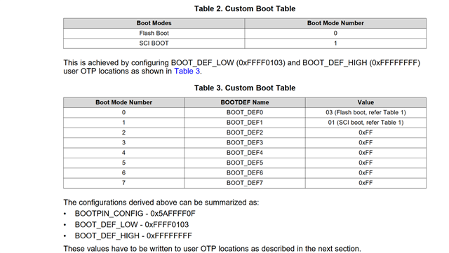
I am working from the app note SPRACN1, which is basically a variant of boot to SCIA by reading a single gpio pin. If the pin is high then SCIA boot is selected. To test the operation I have a short program that calls reset and reboots according to the boot pin state. If the input is low the program runs repeatedly, if high it stops running, from which I infer it it in SCIA boot mode. I put scope probes on the SCIA pins and started serial_flash_programmer. It is sending an 'a' but my board does not respond (I verified the port with a com terminal). Maybe the app note is missing something but I think I have the Z2 OTP setup correctly, at least it apparently changes the boot mode. My biggest suspicion (that Charles suggested earlier) is that the OTP addresses are not right.

The app code:

#include "driverlib.h"
#include "device.h"
#include "string.h"

// Per SPRACN1
#pragma RETAIN(otp_z2_data)
#pragma DATA_SECTION(otp_z2_data,"dcsm_zsel_z2_1");
const long otp_z2_data = 0x5AFFFF0F;
#pragma RETAIN(otp_z2_data_2)
#pragma DATA_SECTION(otp_z2_data_2,"dcsm_zsel_z2_2");
const long otp_z2_data_2 = 0xFFFF0103;
// End SPRACN1

void setup(void);
void scibFlush(void);
void txb(char* s);

void main(void)
{
    uint32_t in = 0;
    setup();
    txb("\r\nStart:");
    GPIO_setDirectionMode(57U, GPIO_DIR_MODE_IN);

   in = GPIO_readPin(57U);
    txb(in == 1 ? "\nHi" : "\nLow");  //Write to SCI B and flush.
    SysCtl_resetDevice();
    return 0;
}

Here are the link cmd file insertions:

MEMORY
{
	PAGE 0:
	DCSM_ZSEL_Z2_P0: origin = 0x078208, length = 0x000002
	DCSM_ZSEL_Z2_P1: origin = 0x07820C, length = 0x000002
	//DCSM_ZSEL_Z1_P0: origin = 0x07800C, length = 0x000002
	//DCSM_ZSEL_Z1_P1: origin = 0x07801C, length = 0x000002
}

SECTIONS
{
	dcsm_zsel_z2_1 : > DCSM_ZSEL_Z2_P0, PAGE = 0
	dcsm_zsel_z2_2 : > DCSM_ZSEL_Z2_P1, PAGE = 0
}

MEMORY
{ ...

  • Hey John,

    Charles' suspicion appears to be the case. This is the default .cmd generated by the SysConfig DCSM Tool for F2838x:

    /* this linker command file is to be included if user wants to use the DCSM feature on the device
    * DCSM means Dual Zone Code Security Module.
    * This linker command file works as an addendum ot the already existing Flash/RAM linker command file
    * that the project has.
    * The sections in the *_ZoneSelectBlock.asm source file is linked as per the commands given in the file
    * NOTE - please note fill=0xFFFF, this helps if users include this file in the project by mistake and
    * doesn't provide the needed proper *_ZoneSelectBlock.asm sources .
    * Please refer to the Blinky DCSM example in the controlsuite examples for proper usage of this.
    *
    * Once users are confident that they want to program the passwords in OTP, the DSECT section type can be removed.
    *
    */

    MEMORY
    {
    PAGE 0 : /* Program Memory */

    /* Z1 OTP. Z1 password locations / Flash and RAM partitioning */
    DCSM_OTP_Z1_LINKPOINTER : origin = 0x78000, length = 0x00006
    DCSM_OTP_Z1_JLM_ENABLE : origin = 0x78006, length = 0x00002
    DCSM_OTP_Z1_GPREG : origin = 0x78008, length = 0x00008
    DCSM_OTP_Z1_PSWDLOCK : origin = 0x78010, length = 0x00002
    DCSM_OTP_Z1_CRCLOCK : origin = 0x78012, length = 0x00002
    DCSM_OTP_Z1_JTAG_PSWDH : origin = 0x78014, length = 0x00004
    DCSM_OTP_Z1_CMAC_KEY : origin = 0x78018, length = 0x00008

    /* DCSM Z1 Zone Select Contents (!!Movable!!) */
    DCSM_ZSEL_Z1_P0 : origin = 0x78020, length = 0x000020

    /* Z2 OTP. Z2 password locations / Flash and RAM partitioning */
    DCSM_OTP_Z2_LINKPOINTER : origin = 0x78200, length = 0x00006
    DCSM_OTP_Z2_RSVD : origin = 0x78206, length = 0x00002
    DCSM_OTP_Z2_GPREG : origin = 0x78208, length = 0x00008
    DCSM_OTP_Z2_PSWDLOCK : origin = 0x78210, length = 0x00002
    DCSM_OTP_Z2_CRCLOCK : origin = 0x78212, length = 0x00002
    DCSM_OTP_Z2_RSVD1 : origin = 0x78214, length = 0x0000C

    /* DCSM Z2 Zone Select Contents (!!Movable!!) */
    DCSM_ZSEL_Z2_P0 : origin = 0x78220, length = 0x000020

    }

    SECTIONS
    {
    dcsm_otp_z1_linkpointer : > DCSM_OTP_Z1_LINKPOINTER PAGE = 0
    dcsm_otp_z1_gpreg : > DCSM_OTP_Z1_GPREG PAGE = 0, type = DSECT
    dcsm_otp_z1_pswdlock : > DCSM_OTP_Z1_PSWDLOCK PAGE = 0
    dcsm_otp_z1_crclock : > DCSM_OTP_Z1_CRCLOCK PAGE = 0
    dcsm_otp_z1_jlm_enable : > DCSM_OTP_Z1_JLM_ENABLE, PAGE = 0
    dcsm_otp_z1_jtag_pswdh : > DCSM_OTP_Z1_JTAG_PSWDH, PAGE = 0, type = DSECT
    dcsm_otp_z1_cmac_key : > DCSM_OTP_Z1_CMAC_KEY, PAGE = 0, type = DSECT
    dcsm_zsel_z1 : > DCSM_ZSEL_Z1_P0 PAGE = 0

    dcsm_otp_z2_linkpointer : > DCSM_OTP_Z2_LINKPOINTER PAGE = 0
    dcsm_otp_z2_gpreg : > DCSM_OTP_Z2_GPREG PAGE = 0, type = DSECT
    dcsm_otp_z2_pswdlock : > DCSM_OTP_Z2_PSWDLOCK PAGE = 0
    dcsm_otp_z2_crclock : > DCSM_OTP_Z2_CRCLOCK PAGE = 0
    dcsm_rsvd_z2 : > DCSM_OTP_Z2_RSVD, PAGE = 0, type = DSECT
    dcsm_rsvd1_z2 : > DCSM_OTP_Z2_RSVD1, PAGE = 0, type = DSECT
    dcsm_zsel_z2 : > DCSM_ZSEL_Z2_P0 PAGE = 0
    }

    /*
    //===========================================================================
    // End of file.
    //===========================================================================
    */

  • Thanks Luke, I think...

    I appreciate it but it looks like a big pill to swallow, definitely out of my comfort zone.

    I am looking for examples. The notes at the top of the file above state:

    Please refer to the Blinky DCSM example in the controlsuite examples for proper usage of this. I have not found anything called control suite in all of C2000.

    Is there such a set of examples?

    I did find

    C:\ti\c2000\C2000Ware_4_01_00_00\driverlib\f2838x\F28386 Examples\c28x\led\led_ex2_blinky_dcsm.c. Unsure if this will work for c28x_dual.

    I will gnaw on this a while but I am sure I will be back.

    Thanks again.

  • I thought I would start with the sysconfig tool to see what I could setup. A couple of  problems right away.

    1) Under password lock the choices are enable or disable permanently. I do not want to do either permanently at this point.

    2) Under Z2 boot settings there are pairs for SCIA, one is gpio84 tx and gpio85 rx. We use gpio9 for rx but this choice is not available.

  • Hey John,

    Apologies for the dump of information. I only meant to point out the default value for DCSM_ZSEL_Z2_P0 : origin = 0x78220, length = 0x000020.

    Looking at your code more closely, it looks like you have the correct addresses for configuring GPREG1 and GPREG3, I originally thought you were attempting to configure the zone select block.

    I believe SysConfig allows you to disable password lock temporarily, only the the enable option should be permanent, let me verify this with other SysConfig/DCSM experts.

    GPIO8 for TX and GPIO9 for RX should be available options in SysConfig. What C2000Ware and CCS version are you using?

    When I select this option in SysConfig, my GPREG3 value is set to 0xFFFFC103, however you have it set as 0xFFFF0103, which would correspond to SCIATX=GPIO29 and SCIARX=GPIO28. This may be the cause of your issue.

  • Thanks for the note.Not to worry about the dump. Once I got the config tool straightened out by fixing my project settings it started to make more sense.

    So my link cmd file would be OK if I changed DCSM_ZSEL_Z2_P0 to 0x78220, length = 0x000020.

    We are using CCS 11 and C2000Ware_4_01_00_00. I think I would be allowed to switch to CCS12 if need be.

    I do not see an option for temporary password lock disable unless it is encoded in Linkpointer section.

    The 0xFFFF0103 value was taken in foolish blind faith straight from the app note SPRACN1:

    But I don't think the app note said anything explicit about setup of SCIA pins. So I was flying blind there.  I just found this in the short reference manual, SPRSP14D.

    So it looks like I cannot choose 84 and 9, it must be 84 and 85.

  • Hi John,

    0x78220 is the base address for zone select block 1 for zone 2. The general purpose registers(GPREG) are used to configure boot settings. By using addresses 0x78208 and 0x7820C, you configured GPREG1 and GPREG3 to use GPIO15 as your boot mode select pin and to use GPIO28 and GPIO29 as your SCI boot pins when GPIO15 is driven high. The OTP configurations and their address are listed in this figure in the DCSM chapter. 

  • You're correct that you must use one of the pairs listed in Table 8-19. Were you able to test using GPIO29=SCIATX and GPIO28=SCIARX for SCI boot? To clarify, bits 15-8 in GPREG3 determine the boot mode when using boot mode 1(GPIO15 = 1 in this case). Bits 7-0 control boot 0 which is 0x03 by default(boot from flash).

  • Hi Luke,

    The image is fuzzy and blowing it up does not help. What document is that from please?

    I am not able to test at this time as all of our gpio pins are assigned to other hardware.

    Our board uses gpio 84 for tx and 9 for rx on SCIA and getting the board re-spun is pretty much a non-starter so I need to find a workaround.

    It looks like some/all of the serial_flash_programmer is available. What I propose is to have the flash kernel code resident on my board as a callable function from a maintenance menu. Then modify the serial_flash_programmer to skip downloading the flash kernel, skip autobaud and run at 9600, then proceed with transferring the CPU1 and CM files.

    Does that seem practical or doable?

    Thanks,

    John

  • Hey John,

    This image is from the DCSM chapter in the F2838x manual.

    Let me loop in our serial flash programmer and boot-ROM experts, they would be more capable of helping with this question.

  • Hi John,

    If you want the flash kernel resident on the board, what you could do is change the linker cmd file so that the kernel resides in flash memory, that way you only have to download it once and save it for sector of your choosing. By skipping autobaud you are fine to run at 9600 if your setup allows. This seems doable. 

    Will look into this more tomorrow.

    Thanks,
    Charles

  • Looking forward to your followup.

    JH

  • Hi John,

    For the F28386S, what you could do is to modify the Flash_API_lnk.cmd file and modify it so that the sections are aligned to flash for the kernel purposes. Then, the build configuration, including renaming.

    https://e2e.ti.com/cfs-file/__key/communityserver-discussions-components-files/171/2838x_5F00_flash_5F00_api_5F00_lnk.cmd

    I still need a bit more time to look at this. 

    Thanks,

    Charles

  • I would like to emulate the SCIA boot mode code. One of the serial flash programmer README files states: "The boot loader of the device copies the incoming data into RAM, then branches to the specified entry point."

    Can this  load and entry point be determined?