


Part Number: TMS320F280025C
Other Parts Discussed in Thread: C2000WARE
Hi team,
I am very new to TMS320F280025c microcontroller. In my project I wanted to use LIN communication in SCI mode with DMA and wanted to view the data bytes in putty terminal.
The program I found from the example code of "C2000Ware_4_02_00_00\driverlib\f28002x\examples\lin\lin_ex3_sci_dma.c "
I found that GPIO_22 and GPIO_23 pins are used for LIN_tx and LIN_rx respectively. So, I configure those pins and disable the internal loopback mode. For the transmission, I only sent two bytes of char data and did some modifications. In oscilloscope, I observed a single pulse is being triggered via GPIO_22 pin after a DMA transmission request but didn't find any data bits or other pulses.
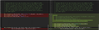
The modified code, I am attaching herewith. Your help would relief me out of the burden. Please help me out.
//#############################################################################
 //
 // FILE:   lin_ex3_sci_dma.c
 //
 // TITLE:  LIN SCI MODE Internal Loopback with DMA
 //
 //! \addtogroup driver_example_list
 //! <h1> LIN SCI MODE Internal Loopback with DMA </h1>
 //!
 //! This example configures the LIN module in SCI mode for internal loopback
 //! with the use of the DMA. The LIN module performs as SCI with a set
 //! character and frame length in multi-buffer mode. When the transmit buffers
 //! in the LINTD0 and LINTD1 registers have enough space, the DMA will transfer
 //! data from global variable sData into those transmit registers. Once the
 //! received buffers in the LINRD0 and LINRD1 registers contain data,the DMA
 //! will transfer the data into the global variable rdata.
 //!
 //! When all data has been placed into rData, a check of the validity of the
 //! data will be performed in one of the DMA channels' ISRs.
 //!
 //! \b External \b Connections \n
 //!  - None
 //!
 //! \b Watch \b Variables \n
 //!  - \b sData - Data to send
 //!  - \b rData - Received data
 //!
 //
 //#############################################################################
 //
 //
 // $Copyright:
 // Copyright (C) 2022 Texas Instruments Incorporated - http://www.ti.com/
 //
 // Redistribution and use in source and binary forms, with or without
 // modification, are permitted provided that the following conditions
 // are met:
 //
 //   Redistributions of source code must retain the above copyright
 //   notice, this list of conditions and the following disclaimer.
 //
 //   Redistributions in binary form must reproduce the above copyright
 //   notice, this list of conditions and the following disclaimer in the
 //   documentation and/or other materials provided with the
 //   distribution.
 //
 //   Neither the name of Texas Instruments Incorporated nor the names of
 //   its contributors may be used to endorse or promote products derived
 //   from this software without specific prior written permission.
 //
 // THIS SOFTWARE IS PROVIDED BY THE COPYRIGHT HOLDERS AND CONTRIBUTORS
 // "AS IS" AND ANY EXPRESS OR IMPLIED WARRANTIES, INCLUDING, BUT NOT
 // LIMITED TO, THE IMPLIED WARRANTIES OF MERCHANTABILITY AND FITNESS FOR
 // A PARTICULAR PURPOSE ARE DISCLAIMED. IN NO EVENT SHALL THE COPYRIGHT
 // OWNER OR CONTRIBUTORS BE LIABLE FOR ANY DIRECT, INDIRECT, INCIDENTAL,
 // SPECIAL, EXEMPLARY, OR CONSEQUENTIAL DAMAGES (INCLUDING, BUT NOT
 // LIMITED TO, PROCUREMENT OF SUBSTITUTE GOODS OR SERVICES; LOSS OF USE,
 // DATA, OR PROFITS; OR BUSINESS INTERRUPTION) HOWEVER CAUSED AND ON ANY
 // THEORY OF LIABILITY, WHETHER IN CONTRACT, STRICT LIABILITY, OR TORT
 // (INCLUDING NEGLIGENCE OR OTHERWISE) ARISING IN ANY WAY OUT OF THE USE
 // OF THIS SOFTWARE, EVEN IF ADVISED OF THE POSSIBILITY OF SUCH DAMAGE.
 // $
 //#############################################################################

 //
 // Included Files
 //
 #include "driverlib.h"
 #include "device.h"

 //
 // Defines
 //
//Modified
 // #define BURST       4
// #define TRANSFER    32
// #define CHAR_LENGTH     8
// #define FRAME_LENGTH    8

#define BURST       1
#define TRANSFER    1
#define CHAR_LENGTH     8
#define FRAME_LENGTH    1

 //
 // Configure the Baud Rate to 115.207kHz
 //
 uint32_t PRESCALER=0x000001a;
 uint16_t DIVIDER=0x0002;

 //
 // Globals
 //
 //Modified
  uint16_t sData[2] = {'a', 'b'};
  uint16_t rData[2];
// unsigned char *sData;
// unsigned char *rData;

 //Place buffers in GSRAM
 #pragma DATA_SECTION(sData, "ramgs0");
 #pragma DATA_SECTION(rData, "ramgs0");

 volatile uint16_t done = 0;         // Flag to set when all data transfered

 //
 // Function Prototypes
 //
 void initDMA(void);
 void configureSCIMode(void);
 __interrupt void dmaCh5ISR(void);
 __interrupt void dmaCh6ISR(void);


 //
 // Main
 //
 void main(void)
 {
     //
     // Initialize device clock and peripherals
     //
     Device_init();

     //
     // Initialize GPIO
     //
     Device_initGPIO();

     // Pin config for LIN tx and LIN rx
     GPIO_setPinConfig(DEVICE_GPIO_CFG_LINTXA);
     GPIO_setPinConfig(DEVICE_GPIO_CFG_LINRXA);
     // GPIO_23 is used as LINTXA
     GPIO_setDirectionMode(23, GPIO_DIR_MODE_IN);
     GPIO_setPadConfig(23, GPIO_PIN_TYPE_PULLUP);
     GPIO_setQualificationMode(23, GPIO_QUAL_ASYNC);
     // GPIO_23 is used as LINRXA
     GPIO_setDirectionMode(22, GPIO_DIR_MODE_OUT);
     GPIO_setPadConfig(22, GPIO_PIN_TYPE_STD);
     GPIO_setQualificationMode(22, GPIO_QUAL_ASYNC);


     //
     // Initialize PIE and clear PIE registers. Disables CPU interrupts.
     //
     Interrupt_initModule();

     //
     // Initialize the PIE vector table with pointers to the shell Interrupt
     // Service Routines (ISR).
     //
     Interrupt_initVectorTable();
     EINT;
     ERTM;

     //
     // Interrupts that are used in this example are re-mapped to
     // ISR functions found within this file.
     // This registers the interrupt handler in PIE vector table.
     //
     Interrupt_register(INT_DMA_CH5, &dmaCh5ISR);
     Interrupt_register(INT_DMA_CH6, &dmaCh6ISR);

     //
     // Enable the DMA interrupt signals
     //
     Interrupt_enable(INT_DMA_CH5);
     Interrupt_enable(INT_DMA_CH6);

     //
     // Initialize the DMA
     //
     initDMA();

     //
     //Initialize the LIN Module
     //
     LIN_initModule(LINA_BASE);

     //
     // Configure the LIN module to operate in SCI mode
     //
     configureSCIMode();

     //
     // Initialize the data buffers
     //
//Modified
//     for(i = 0; i < 128; i++)
//     {
//        sData[i]= i;
//        rData[i]= 0;
//     }

     //
     // Wait for the SCI receiver to be idle
     //
     while(!LIN_isSCIReceiverIdle(LINA_BASE));

     //
     // Wait until space is available in the transmit buffer.
     //
     while(!LIN_isSCISpaceAvailable(LINA_BASE)){}
     //
     //Initiate transfer through a CPU write
     //
     LIN_sendData(LINA_BASE,(unsigned int*)0xFFFF);

     //
     // Start the DMA receive channel
     //
     DMA_startChannel(DMA_CH6_BASE);

     //
     //Start the DMA transmit channel
     //
     DMA_startChannel(DMA_CH5_BASE);

     //Write one data byte when Tx buffer is ready
     LIN_writeSCICharBlocking(LINA_BASE, sData[1]);
     //
     //Wait until the DMA transfer is complete
     //
//     while(!done);


     //
     //When the DMA transfer is complete the program will stop here
     //
     ESTOP0;

 }

 //
 // Function to configure LIN in SCI Mode
 //
 void
 configureSCIMode(void)
 {
     //
     // Enter LIN reset state to perform configurations
     //
     LIN_enterSoftwareReset(LINA_BASE);

     //
     // Switch LIN into SCI mode
     //
     LIN_enableSCIMode(LINA_BASE);

     //
     // Set the SCI communication mode to idle line
     //
     LIN_setSCICommMode(LINA_BASE, LIN_COMM_SCI_IDLELINE);

     //
     // Set SCI to transmit one stop bit
     //
     LIN_setSCIStopBits(LINA_BASE,LIN_SCI_STOP_ONE);

     //
     // Disable parity check
     //
     LIN_disableSCIParity(LINA_BASE);

//Modified
     //
     // Enable multi-buffer mode
     //
//     LIN_enableMultibufferMode(LINA_BASE);

     //
     // Module set to complete operations when halted by debugger
     //
     LIN_setDebugSuspendMode(LINA_BASE, LIN_DEBUG_COMPLETE);

     //
     // Set character length as 8-bits
     //
     LIN_setSCICharLength(LINA_BASE, CHAR_LENGTH);

     //
     // Set to 1 character in response field
     //
     LIN_setSCIFrameLength(LINA_BASE, FRAME_LENGTH);

     //
     // Set the Baud Rate
     //
     LIN_setBaudRatePrescaler(LINA_BASE, PRESCALER, DIVIDER);

//Modified
     //
     // Enable Internal Loopback mode
     //
//     LIN_enableIntLoopback(LINA_BASE);
//     LIN_disableIntLoopback(LINA_BASE);
     //
     //Enable the DMA for transmission
     //
     LIN_enableSCIInterrupt(LINA_BASE, LIN_SCI_INT_TX_DMA);

     //
     //Enable the DMA to receive
     //
     LIN_enableSCIInterrupt(LINA_BASE, LIN_SCI_INT_RX_DMA);


     // Exit LIN reset state
     //
     LIN_exitSoftwareReset(LINA_BASE);
 }

 //
 // DMA setup for both TX and RX channels.
 //
 void initDMA()
 {
     //
     // Initialize DMA
     //
     DMA_initController();

     //
     // Configure DMA Ch5 for TX. When there is enough space in the buffers found in
     // the LINTD0 and LINTD1 registers, data will be transferred from the sdata buffer
     // to the LIN's transmit registers. The destination address is configured to start
     // in the most significant part of the LINTD1 register (TD4/TD5 transmit buffers)and
     // move two address's down with every burst until it fills up the least significant
     // part of the LINTD0 register (TD2/ TD3 transmit buffers).After every transfer of
     // 4 bursts the destination address is brought back to the address of the TD4/TD5
     // buffers contained in the LINTD1 register.
     //

//Modified
//     DMA_configAddresses(DMA_CH5_BASE, (uint16_t *)(LINA_BASE + LIN_O_TD1+2), sData);
//     DMA_configBurst(DMA_CH5_BASE, BURST, 1, -2);
//     DMA_configTransfer(DMA_CH5_BASE, TRANSFER, 1, 6);
//     DMA_configMode(DMA_CH5_BASE, DMA_TRIGGER_LINATX, DMA_CFG_ONESHOT_DISABLE |
//                    DMA_CFG_CONTINUOUS_DISABLE | DMA_CFG_SIZE_16BIT);


     DMA_configAddresses(DMA_CH5_BASE, (uint16_t *)(LINA_BASE + LIN_O_SCITD), sData);
     DMA_configBurst(DMA_CH5_BASE, BURST, 0, 0);
     DMA_configTransfer(DMA_CH5_BASE, TRANSFER, 0, 0);
     DMA_configMode(DMA_CH5_BASE, DMA_TRIGGER_LINATX, DMA_CFG_ONESHOT_DISABLE |
                    DMA_CFG_CONTINUOUS_DISABLE | DMA_CFG_SIZE_16BIT);

     //
     // Configure DMA Ch5 interrupts
     //
     DMA_setInterruptMode(DMA_CH5_BASE, DMA_INT_AT_END);
     DMA_enableInterrupt(DMA_CH5_BASE);
     DMA_enableTrigger(DMA_CH5_BASE);

     //
     // Configure DMA Ch6 for RX. When the buffers found in the LINRD0 and LINRD1
     // registers are full, data will be transferred to the rdata buffer. The source
     // address is configured to start in the most significant part of the LINRD1
     // register (RD4/RD5 receive buffers) and move two address's down with every
     // burst until it transfers the least significant part of the LINTD0 register
     // (RD2/ RD3 receive buffers).After every transfer of 4 bursts the source
     // address is brought back to the address of the RD4/RD5 buffers contained in
     // the LINRD1 register.
     //

//Modified
//     DMA_configAddresses(DMA_CH6_BASE, rData,(uint16_t *)(LINA_BASE + LIN_O_RD1+2));
//     DMA_configBurst(DMA_CH6_BASE, BURST, -2, 1);
//     DMA_configTransfer(DMA_CH6_BASE, TRANSFER, 6, 1);
//     DMA_configMode(DMA_CH6_BASE, DMA_TRIGGER_LINARX, DMA_CFG_ONESHOT_DISABLE |
//                    DMA_CFG_CONTINUOUS_DISABLE | DMA_CFG_SIZE_16BIT);

     DMA_configAddresses(DMA_CH6_BASE, rData,(uint16_t *)(LIN_O_SCIRD));
     DMA_configBurst(DMA_CH6_BASE, BURST, 0, 0);
     DMA_configTransfer(DMA_CH6_BASE, TRANSFER, 0, 0);
     DMA_configMode(DMA_CH6_BASE, DMA_TRIGGER_LINARX, DMA_CFG_ONESHOT_DISABLE |
                    DMA_CFG_CONTINUOUS_DISABLE | DMA_CFG_SIZE_16BIT);

     //
     // Configure DMA Ch6 interrupts
     //
     DMA_setInterruptMode(DMA_CH6_BASE, DMA_INT_AT_END);
     DMA_enableInterrupt(DMA_CH6_BASE);
     DMA_enableTrigger(DMA_CH6_BASE);
 }

 //
 // DMA Channel 5 ISR
 //
 __interrupt void dmaCh5ISR(void)
 {
     DMA_stopChannel(DMA_CH5_BASE);
     Interrupt_clearACKGroup(INTERRUPT_ACK_GROUP7);
     return;
//     done = 1;
 }

 //
 // DMA Channel 6 ISR
 //
  __interrupt void dmaCh6ISR(void)
 {
     uint16_t i;
     DMA_stopChannel(DMA_CH6_BASE);
     Interrupt_clearACKGroup(INTERRUPT_ACK_GROUP7);

//Modified
 //    //
 //    //Check for data integrity
 //    //
 //    for(i=0; i<128; i++)
 //    {
 //        if(rData[i] !=i)
 //        {
 //           //Something went wrong, rdata doesn't contain expected data.
 //           ESTOP0;
 //        }
 //    }

//     done = 1;
     return;
 }


 '
'
